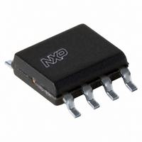
TDA8541T/N1,112 NXP Semiconductors, TDA8541T/N1,112 Datasheet - Page 6

TDA8541T/N1,112
Manufacturer Part Number
TDA8541T/N1,112
Description
IC AMP AUDIO PWR 1.2W MONO 8SOIC
Manufacturer
NXP Semiconductors
Type
Class ABr
Datasheet
1.TDA8541TN1118.pdf
(18 pages)
Specifications of TDA8541T/N1,112
Output Type
1-Channel (Mono)
Package / Case
8-SOIC (3.9mm Width)
Max Output Power X Channels @ Load
1.2W x 1 @ 8 Ohm
Voltage - Supply
2.2 V ~ 18 V
Features
Depop, Mute, Short-Circuit and Thermal Protection, Standby
Mounting Type
Surface Mount
Product
Class-AB
Output Power
1.2 W
Available Set Gain
30 dB
Thd Plus Noise
0.15 %
Operating Supply Voltage
5 V
Supply Current
8 mA
Maximum Power Dissipation
800 mW
Maximum Operating Temperature
+ 85 C
Mounting Style
SMD/SMT
Audio Load Resistance
8 Ohms
Input Bias Current (max)
500 nA
Input Signal Type
Differential or Single
Minimum Operating Temperature
- 40 C
Output Signal Type
Differential, Single
Supply Type
Single
Supply Voltage (max)
18 V
Supply Voltage (min)
2.2 V
Lead Free Status / RoHS Status
Lead free / RoHS Compliant
Other names
568-3475-5
935211650112
TDA8541TD
935211650112
TDA8541TD
NXP Semiconductors
TEST AND APPLICATION INFORMATION
Test conditions
Because the application can be either Bridge-Tied Load
(BTL) or Single-Ended (SE), the curves of each application
are shown separately.
The thermal resistance = 100 K/W for the DIP8 envelope;
the maximum sine wave power dissipation for
T
For T
BTL application
T
f = 1 kHz, R
22 Hz to 22 kHz.
The BTL application diagram is shown in Fig.3.
The quiescent current has been measured without any
load impedance. The total harmonic distortion as a
function of frequency was measured with a low-pass filter
of 80 kHz. The value of capacitor C2 influences the
behaviour of the SVRR at low frequencies, increasing the
value of C2 increases the performance of the SVRR.
The figure of the mode select voltage (V
of the supply voltage shows three areas; operating, mute
and standby. It shows, that the DC-switching levels of the
mute and standby respectively depends on the supply
voltage level.
1998 Apr 01
150 25
--------------------- -
150 60
--------------------- -
amb
amb
1 W BTL audio amplifier
100
100
–
–
= 25 °C is:
= 25 °C if not specially mentioned, V
amb
= 60 °C the maximum total power dissipation is:
=
=
L
1.25 W
0.9 W
= 8 Ω, G
.
.
v
= 20 dB, audio band-pass
ms
CC
) as a function
= 5 V,
6
SE application
T
f = 1 kHz, R
22 Hz to 22 kHz.
The SE application diagram is shown in Fig.13.
The capacitor value of C3 in combination with the load
impedance determines the low frequency behaviour.
The total harmonic distortion as a function of frequency
was measured with low-pass filter of 80 kHz. The value of
capacitor C2 influences the behaviour of the SVRR at low
frequencies, increasing the value of C2 increases the
performance of the SVRR.
General remark
The frequency characteristic can be adapted by
connecting a small capacitor across the feedback resistor.
To improve the immunity of HF radiation in radio circuit
applications, a small capacitor can be connected in parallel
with the feedback resistor (56 kΩ); this creates a low-pass
filter.
amb
= 25 °C if not specially mentioned, V
L
= 4 Ω, G
v
= 20 dB, audio band-pass
Product specification
TDA8541
CC
= 7.5 V,


