LMV1088RL/NOPB National Semiconductor, LMV1088RL/NOPB Datasheet
LMV1088RL/NOPB
Specifications of LMV1088RL/NOPB


Related parts for LMV1088RL/NOPB

LMV1088RL/NOPB Summary of contents
Page 1
... The dual microphone inputs are differential to provide excel- lent noise immunity. The microphones are biased with an internal low-noise bias supply. Application of the LMV1088 PowerWise® registered trademark of National Semiconductor Corporation. © 2009 National Semiconductor Corporation LMV1088 Key Specifications (3.3V supply, unless otherwise specified) ■ ...
Page 2
Typical Application www.national.com 2 ...
Page 3
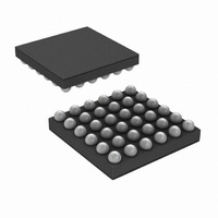
Connection Diagrams 36 Bump micro SMD Marking Top View X = Plant Code YY = Date Code TT = Die Tracability ZA1 = LMV1088RL 36 Bump micro SMD package Top View Order Number LMV1088RL See NS Package Number RLA36TTA 20213031 ...
Page 4
Pin Descriptions Bump Pin Name Number MIC2– A5 MIC2+ A6 Mic Bias GND MIC1 ...
Page 5
... Absolute Maximum Ratings If Military/Aerospace specified devices are required, please contact the National Semiconductor Sales Office/ Distributors for availability and specifications. Supply Voltage Storage Temperature ESD Rating (Note 7) ESD Rating (Note 8) Junction Temperature (T ) JMAX Mounting Temperature Infrared or Convection (20 sec.) Electrical Characteristics 3.3V and 5.0V Unless otherwise specified, all limits guaranteed for T 11), preamplifier gain = 20dB, postamplifier gain = -2 ...
Page 6
Supply Current during Calibration and I DDCP Programming I Supply Current DD Digital Interface Characteristics Unless otherwise specified, all limits guaranteed for T Symbol Parameter V Logic High Input Level IH V Logic Low Input Level IL ts CAL Setup ...
Page 7
Typical Performance Characteristics , pass through mode (Note 11), preamplifier gain = 20dB, postamplifier gain = –2.5dB Supply Current vs. Supply Voltage THD+N vs Frequency, pass through mode Mic2 V = 36mV IN P-P THD+N vs Frequency, Noise ...
Page 8
THD pass through mode Mic2 IN THD Noise canceling mode IN Mic1 AC shorted, signal at Mic2 PSRR vs Frequency, pass through mode Mic2 Mic1+ Mic2 AC shorted www.national.com THD signal ...
Page 9
PSRR vs Frequency, Microphone Bias Mic1+ Mic2 AC shorted 20213022 9 www.national.com ...
Page 10
Application Data Gain Balance and Gain Budget In systems where input signals have a high dynamic range, critical noise levels and where the dynamic range of the output voltage is also limited, careful gain balancing can be essential EXAMPLE1 An ...
Page 11
Chip Address Adress=' Chip Address Adress=' DATA VALIDITY The data on SDA line must be stable during the HIGH period of the clock signal (SCL). In other ...
Page 12
Register changes take effect at the SCL rising edge during the last acknowledge (ACK ) from slave write (SDA = “0” read (SDA = “1”) ack = acknowledge (SDA pulled down by slave repeated ...
Page 13
Symbol 1 Hold Time (repeated) START Condition 2 Clock Low Time 3 Clock High Time 4 Setup Time for a Repeated START Condition 5 Data Hold Time (Output direction, delay generated by LMV1088) 5 Data Hold Time (Input direction, delay ...
Page 14
Address Reg. Bits 0x01h A [3:0] Microphone preamplifier gain from 6dB up to 36dB in 2dB steps. 0000 0001 0010 0011 0100 0101 0110 0111 1000 1001 1010 1011 1100 1101 1110 1111 A4 = Mute mic1 and A5 = ...
Page 15
Address Reg. Bits 0x0Fh O [7:4] Control the gain compensation between the two mics at 300Hz (Note 1) 0000 (0) 0001 (1) 0010 (2) 0011 (3) 0100 (4) 0101 (5) 0110 (6) 0111 (7) 1000 (8) 1001 (9) 1010 (A) ...
Page 16
Address Reg. Bits 0x10h P [7:4] Control compensation gain for Mic2 channel at ALL frequencies (Note 1) 0000 (0) 0001 (1) 0010 (2) 0011 (3) 0100 (4) 0101 (5) 0110 (6) 0111 (7) 1000 (8) 1001 (9) 1010 (A) 1011 ...
Page 17
Automatic Calibration The full automatic calibration should only be required once, when the product containing the LMV1088 has completed manufacture, and prior to application packaging. The product containing the LMV1088 will be calibrated to the micro- phones, the microphone spacings, ...
Page 18
PERFORMING A THREE TONE CALIBRATION In a system with two microphones in an enclosure there will always be a difference in the transfer function in both gain and frequency response. The LMV1088 has the capability to per- form an automatic ...
Page 19
THREE TONE CALIBRATION SETUP A calibration test setup consist of a test room (acoustical box) with a loudspreaker (acoustical source) driven with the test tone sequence from Figure 8. The test setup is shown in Fig- ure 9. The distance ...
Page 20
Manual Calibration You can manually program the gain of the two mic inputs on the LMV1088 using the interface. Table 5 shows the con- trol bits for Register O and P with the corresponding ...
Page 21
Measurement Setup Because of the nature of the calibration system it is not pos- sible to predict the absolute gain in the two microphone channels of the Far Field Noise Cancelling System. This is because, after the calibration function has ...
Page 22
MEASURING NOISE AND SNR The overall noise of the LMV1088 is measured within the fre- quency band from 10Hz to 22kHz using an A-weighted filter. For the signal to noise ratio (SNR) the signal level at the out- put is ...
Page 23
Revision History Rev Date 1.0 09/26/07 1.01 12/10/07 1.02 03/07/08 1.03 03/10/08 1.04 03/12/08 1.05 03/14/08 1.06 03/25/08 1.07 03/28/08 1.08 04/04/08 1.09 04/17/08 1.10 05/27/08 1.11 06/05/08 1.12 09/19/08 1.13 02/11/09 1.14 02/19/09 1.15 02/26/09 Description Initial release. Few ...
Page 24
Physical Dimensions www.national.com inches (millimeters) unless otherwise noted 36 Bump micro SMD Technology NS Package Number RLA36TTA X = 3.459±0.03 3.459±0.03 0.6±0.075 3 ...
Page 25
25 www.national.com ...
Page 26
... For more National Semiconductor product information and proven design tools, visit the following Web sites at: Products Amplifiers www.national.com/amplifiers Audio www.national.com/audio Clock and Timing www.national.com/timing Data Converters www.national.com/adc Interface www.national.com/interface LVDS www.national.com/lvds Power Management www.national.com/power Switching Regulators www.national.com/switchers LDOs www.national.com/ldo LED Lighting www ...