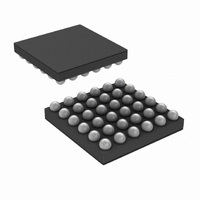
LMV1088RL/NOPB National Semiconductor, LMV1088RL/NOPB Datasheet - Page 11

LMV1088RL/NOPB
Manufacturer Part Number
LMV1088RL/NOPB
Description
IC AMP AUDIO MONO AB MIC 36USMD
Manufacturer
National Semiconductor
Series
PowerWise®r
Type
Class ABr
Datasheet
1.LMV1088RLNOPB.pdf
(26 pages)
Specifications of LMV1088RL/NOPB
Output Type
1-Channel (Mono)
Voltage - Supply
2.7 V ~ 5.5 V
Features
Differential Inputs, I²C, Microphone, Mute
Mounting Type
Surface Mount
Package / Case
36-MicroSMDxt
Amplifier Class
AB
No. Of Channels
2
Supply Voltage Range
2.7V To 5.5V
Load Impedance
10kohm
Operating Temperature Range
-40°C To +85°C
Amplifier Case Style
SMD
No. Of Pins
36
Rohs Compliant
Yes
Lead Free Status / RoHS Status
Lead free / RoHS Compliant
Max Output Power X Channels @ Load
-
Other names
LMV1088RLTR
I
The data on SDA line must be stable during the HIGH period
of the clock signal (SCL). In other words, state of the data line
can only be changed when SCL is LOW.
I
START and STOP bits classify the beginning and the end of
the I
fined as SDA signal transitioning from HIGH to LOW while
SCL line is HIGH. STOP condition is defined as the SDA tran-
sitioning from LOW to HIGH while SCL is HIGH. The I
master always generates START and STOP bits. The I
is considered to be busy after START condition and free after
STOP condition. During data transmission, I
generate repeated START conditions. First START and re-
peated START conditions are equivalent, function-wise.(Note
14)
2
2
C DATA VALIDITY
C START AND STOP CONDITIONS
2
C data transmission session. START condition is de-
2
1
nd
st
I
I
2
2
C Adress='0'
C Adress='1'
Chip Address
Chip Address
I
I
2
2
C Start Stop Conditions
C Signals: Data Validity
D7
1
1
2
C master can
202130q1
TABLE 2. Chip Address
D6
202130q2
2
1
1
C bus
2
C
11
D5
0
0
Note 14: The master should issue STOP after no acknowledgement.
TRANSFERRING DATA
Every byte put on the SDA line must be eight bits long, with
the most significant bit (MSB) being transferred first. Each
byte of data has to be followed by an acknowledge bit. The
acknowledge related clock pulse is generated by the master.
The transmitter releases the SDA line (HIGH) during the ac-
knowledge clock pulse. The receiver must pull down the SDA
line during the 9
receiver which has been addressed must generate an ac-
knowledge after each byte has been received.
After the START condition, the I
dress. This address is seven bits long followed by an eighth
bit which is a data direction bit (R/W). The LMV1088 address
is 11001100
a WRITE and a “1” indicates a READ. The second byte se-
lects the register to which the data will be written. The third
byte contains data to write to the selected register.
D4
0
0
2
or 11001110
th
clock pulse, signifying an acknowledge. A
D3
1
1
I
2
C Chip Address
2
. For the eighth bit, a “0” indicates
D2
1
1
2
C master sends a chip ad-
D1
0
1
www.national.com
W/R
W/R
202130q3
D0


