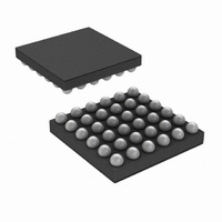
LMV1088RL/NOPB National Semiconductor, LMV1088RL/NOPB Datasheet - Page 10

LMV1088RL/NOPB
Manufacturer Part Number
LMV1088RL/NOPB
Description
IC AMP AUDIO MONO AB MIC 36USMD
Manufacturer
National Semiconductor
Series
PowerWise®r
Type
Class ABr
Datasheet
1.LMV1088RLNOPB.pdf
(26 pages)
Specifications of LMV1088RL/NOPB
Output Type
1-Channel (Mono)
Voltage - Supply
2.7 V ~ 5.5 V
Features
Differential Inputs, I²C, Microphone, Mute
Mounting Type
Surface Mount
Package / Case
36-MicroSMDxt
Amplifier Class
AB
No. Of Channels
2
Supply Voltage Range
2.7V To 5.5V
Load Impedance
10kohm
Operating Temperature Range
-40°C To +85°C
Amplifier Case Style
SMD
No. Of Pins
36
Rohs Compliant
Yes
Lead Free Status / RoHS Status
Lead free / RoHS Compliant
Max Output Power X Channels @ Load
-
Other names
LMV1088RLTR
www.national.com
Application Data
Gain Balance and Gain Budget
In systems where input signals have a high dynamic range,
critical noise levels and where the dynamic range of the output
voltage is also limited, careful gain balancing can be essential
EXAMPLE1
An application using microphones with 50mV
output voltage, and a baseband chip after the LMV1088 with
1.5V
For optimum noise performance we would like to have the
maximum gain at the input stage.
So using Pre Amp gain =14dB and Post Amp gain = 6dB is
the optimum for this application.
1.
2.
3.
4.
5.
6.
7.
So using Pre Amp gain =14dB and Post Amp gain = 6dB is
the optimum for this application.
50mV
This is higher than the maximum 1.4V
Noice cancelling Processor (NCP). This means a gain
lower then 28.9dB should be selected.
Select the nearest lower gain from the gain setting table
to be 28dB. This will prevent the NCP from being
overloaded by the microphone. With this setting, the
resulting output level of the Pre Amplifier will be
1.26V
The NCP can have a maximum processing gain of 9dB
(depending on the calibration result) which will result in
3.5V
then maximum level hat is allowed at the input of the Post
Amp of the LMV1088. Therefore the Pre Amp gain has
to be reduced, to 1.4V
the Pre Amp gain to a maximum of 20dB.
The baseband chip limits the maximum output voltage to
1.5V
results in having a lower level at the input of the Post Amp
of 0.75V
of 9dB the output of the Pre Amp must be <266mV
Calculating the new gain for the Pre Amp will result in
<1.4 dB gain.
The nearest lower gain will be 14dB.
pp
maximum input voltage.
pp
pp
pp
pp
at the output of the LMV1088. This level is higher
with the minimum of 6dB Post Amp gain, this
.
+ 36 dB = 3.1V
pp
. Now calculating this for a maximum NCP gain
pp
pp
minus 9dB = 0.5V
.
pp
allowed for the
FIGURE 2. Maximum Signal Levels
pp
pp
. This limits
maximum
pp
.
10
for the best performance. Having not enough gain in the Pre
Amplifier can result in higher noise levels while to much gain
in the Pre Amplifier will result in clipping and saturation in the
noise cancelling processor and output stages.
The gain ranges and maximum signal levels for the different
functional blocks is shown in Figure 2. Two examples are giv-
en as a guideline how to select proper gain settings.
EXAMPLE 2
An application using microphones with 10mV
output voltage, and a baseband chip after the LMV1088 with
3.3V
For optimum noise performance we would like to have the
maximum gain at the input stage.
1.
2.
3.
4.
5.
So using Pre Amp gain =14dB and Post Amp gain = 6dB is
the optimum for this application.
I
I
The LMV1088 pin Serial Clock (SCL) is used for the I
SCL and the pin Serial Data (SDA) is used for the I
signal SDA. Both of these signals need a pull-up resistor ac-
cording to I
through two slave addresses. The two I
LMV1088 are given inTable 2 .
2
2
C SIGNALS
C Compatible Interface
10mV
This is lower than the maximum 1.4V
The NCP can have a maximum processing gain of 9dB
(depending on the calibration result) which will result in
3.5V
then maximum level hat is allowed at the input of the Post
Amp of the LMV1088. Therefore the Pre Amp gain has
to be reduced, to 1.4V
the Pre Amp gain to a maximum of 34dB.
With a Post Amp gain setting of 6dB the output of the
Post Amp will be 2.8V
The nearest lower Post Amp gain will be 6dB.
pp
maximum input voltage.
pp
pp
2
at the output of the LMV1088. This level is higher
C specification. The LMV1088 can be controlled
+ 36dB = 631mV
pp
pp
which is OK for the baseband.
minus 9dB = 0.5V
pp
.
2
20213037
C slave address for
pp
so this is OK.
pp
pp
. This limits
maximum
2
2
C clock
C data


