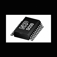
P87LPC769 NXP Semiconductors, P87LPC769 Datasheet - Page 13

P87LPC769
Manufacturer Part Number
P87LPC769
Description
The P87LPC769 is a 20-pin single-chip microcontroller designed forlow pin count applications demanding high-integration, low costsolutions over a wide range of performance requirements
Manufacturer
NXP Semiconductors
Datasheet
1.P87LPC769.pdf
(62 pages)
Available stocks
Company
Part Number
Manufacturer
Quantity
Price
Company:
Part Number:
P87LPC769BD
Manufacturer:
PHILIPS
Quantity:
64
Company:
Part Number:
P87LPC769FD
Manufacturer:
PHILIPS
Quantity:
53
Philips Semiconductors
A/D Timing
The A/D may be clocked in one of two ways. The default is to use
the CPU clock as the A/D clock source. When used in this manner,
the A/D completes a conversion in 31 machine cycles. The A/D may
be operated up to the maximum CPU clock rate of 20 MHz, giving a
conversion time of 9.3 s. The formula for calculating A/D
conversion time when the CPU clock runs the A/D is: 186 s / CPU
clock rate (in MHZ). To obtain accurate A/D conversion results, the
CPU clock must be at least 1 MHz.
The A/D may also be clocked by the on-chip RC oscillator, even if
the RC oscillator is not used as the CPU clock. This is accomplished
by setting the RCCLK bit in ADCON. This arrangement has several
advantages. First, the A/D conversion time is faster at lower CPU
clock rates. Also, the CPU may be run at speeds below 1 MHz
2002 Mar 12
ADCON
Bit addressable
Reset Value: 00h
BIT
ADCON.7
ADCON.6
ADCON.5
ADCON.4
ADCON.3
ADCON.2
ADCON.1, 0
Low power, low price, low pin count (20 pin)
microcontroller with 4 kB OTP 8-bit A/D, and DAC
Address: C0h
AADR1, AADR0
ADCI, ADCS
SYMBOL
AADR1,0
ENDAC1
ENDAC0
ENADC
RCCLK
ADCS
ADCI
0 0
0 1
1 0
1 1
0 0
0 1
1 0
1 1
FUNCTION
When ENADC = 1, the A/D is enabled and conversions may take place. Must be set 10
microseconds before a conversion is started. ENADC cannot be cleared while ADCS or ADCI
are 1.
When ENDAC=1, DAC1 is enabled to provide an analog output voltage. Refer to the section
Digital to Analog Converter (DAC) Outputs for details.
When ENDAC=1, DAC0 is enabled to provide an analog output voltage. Writable while ADCS
and ADCI are 0. Refer to the section Digital to Analog Converter (DAC) Outputs for details.
ENADC and ENDAC0 should not be set at the same time.
A/D conversion complete/interrupt flag. This flag is set when an A/D conversion is completed.
This bit will cause a hardware interrupt if enabled and of sufficient priority. Must be cleared by
software.
A/D start. Setting this bit by software starts the conversion of the selected A/D input. ADCS
remains set while the A/D conversion is in progress and is cleared automatically upon
completion. While ADCS or ADCI are one, new start commands are ignored.
A/D Status
A/D not busy, a conversion can be started.
A/D busy, the start of a new conversion is blocked.
An A/D conversion is complete. ADCI must be cleared prior to starting a new conversion.
An A/D conversion is complete. ADCI must be cleared prior to starting a new conversion. This
state exists for one machine cycle as an A/D conversion is completed.
When RCCLK = 0, the CPU clock is used as the A/D clock. When RCCLK = 1, the internal RC
oscillator is used as the A/D clock. This bit is writable while ADCS and ADCI are 0.
Along with AADR0, selects the A/D channel to be converted. These bits can only be written
while ADCS and ADCI are 0.
A/D Input Selected
AD0 (P0.3).
AD1 (P0.4).
AD2 (P0.5).
AD3 (P0.6).
ENADC ENDAC1 ENDAC0
7
Figure 2. A/D Control Register (ADCON)
6
10
5
When the A/D is operated from the RCCLK while the CPU is running
synchronize A/D operation. The time can range from a minimum of 3
without affecting A/D accuracy. Finally, the Power Down mode may
be used to completely shut down the CPU and its oscillator, along
with other peripheral functions, in order to obtain the best possible
A/D accuracy. This should not be used if the MCU uses an external
clock source greater than 4 MHz.
from another clock source, 3 or 4 machine cycles are used to
machine cycles (at the CPU clock rate) + 108 RC clocks to a
maximum of 4 machine cycles (at the CPU clock rate) + 112 RC
clocks.
Example A/D conversion times at various CPU clock rates are
shown in Table 1. In Table 1, maximum times for RCCLK = 1 use an
ADCI
4
ADCS
3
RCCLK
2
AADR1
1
P87LPC769
AADR0
SU01370
Preliminary data
0


