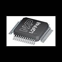
MPT612 NXP Semiconductors, MPT612 Datasheet - Page 5

MPT612
Manufacturer Part Number
MPT612
Description
The MPT612, the first dedicated IC for performing the Maximum Power Point Tracking (MPPT) function, is designed for use in applications that use solar photovoltaic (PV) cells or in fuel cells
Manufacturer
NXP Semiconductors
Datasheet
1.MPT612.pdf
(37 pages)
Available stocks
Company
Part Number
Manufacturer
Quantity
Price
Company:
Part Number:
MPT612FBD48,151
Manufacturer:
ON
Quantity:
22 150
Company:
Part Number:
MPT612FBD48,151
Manufacturer:
NXP Semiconductors
Quantity:
10 000
NXP Semiconductors
Table 2.
MPT612
Product data sheet
Symbol
PIO0 to PIO30
PIO31
PIO0/TXD0/MAT3_1
PIO1/RXD0/MAT3_2
PIO2/SCL0
PIO3/SDA0
PIO4/SCK0
PIO5/MISO0
PIO6/MOSI0
PWMOUT0
PIO8/TXD1/PWMOUT1
PIO9/RXD1/PWMOUT2
PIO10/RTS1/CAP1_0/AD3
Pin description
6.2 Pin description
Pin
16
13
14
18
21
22
23
24
28
29
30
35
[1]
[1]
[2]
[2]
[1]
[1]
[1]
[1]
[1]
[1]
[3]
Type Description
I/O
O
I/O
O
O
I/O
I
O
I/O
I/O
I/O
I/O
I/O
I/O
I/O
I/O
I/O
I/O
O
I/O
O
O
I/O
I
O
I/O
O
I
I
All information provided in this document is subject to legal disclaimers.
PIO0 to PIO30: 31 pins for General Purpose bidirectional digital Input and
Output (GPIO). The operation of these pins is dependent on the selected
pin function.
The functions of pins PIO7, PIO22, PIO23 and PIO24 are not defined as in
the GPIO; do not change these settings.
PIO31 is a digital output pin.
PIO0: general purpose digital input and output pin
TXD0: transmitter output for UART0
MAT3_1: PWM output 1 for timer 3
PIO1: general purpose digital input and output pin
RXD0: receiver input for UART0
MAT3_2: PWM output 2 for Timer 3
PIO2: general purpose digital input and output pin; open-drain output
SCL0: I
PIO3: general purpose digital input and output pin; open-drain output
SDA0: I
PIO4: general purpose digital input and output pin.
SCK0: serial clock for SPI0; SPI clock output from master or input to slave.
PIO5: general purpose digital input and output pin
MISO0: Master In Slave Out for SPI0; data input to SPI master or data
output from SPI slave
PIO6: general purpose digital input and output pin
MOSI0: Master Out Slave In for SPI0; data output from SPI master or data
input to SPI slave
PWMOUT0: PWM output used for switching the device; do not use for
anything else
PIO8: general purpose digital input and output pin
TXD1: Transmitter output for UART1
PWMOUT1: PWM output; same frequency as PWMOUT0, however, the
duty cycle can be changed
PIO9: general purpose digital input and output pin
RXD1: Receiver input for UART1
PWMOUT2: PWM output; same frequency as PWMOUT0, however, the
duty cycle can be changed
PIO10: general purpose digital input and output pin
RTS1: Request To Send output for UART1
CAP1_0: capture input for timer 1, channel 0
AD3: analog-to-digital converter input 3
Rev. 2 — 14 September 2010
2
2
C-bus port 0 clock Input and output; open-drain output
C-bus port 0 data input and output; open-drain output
Maximum power point tracking IC
© NXP B.V. 2010. All rights reserved.
MPT612
5 of 5


