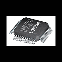
MPT612 NXP Semiconductors, MPT612 Datasheet - Page 8

MPT612
Manufacturer Part Number
MPT612
Description
The MPT612, the first dedicated IC for performing the Maximum Power Point Tracking (MPPT) function, is designed for use in applications that use solar photovoltaic (PV) cells or in fuel cells
Manufacturer
NXP Semiconductors
Datasheet
1.MPT612.pdf
(37 pages)
Available stocks
Company
Part Number
Manufacturer
Quantity
Price
Company:
Part Number:
MPT612FBD48,151
Manufacturer:
ON
Quantity:
22 150
Company:
Part Number:
MPT612FBD48,151
Manufacturer:
NXP Semiconductors
Quantity:
10 000
NXP Semiconductors
[1] 5 V tolerant (if V
[2] Open-drain, 5 V tolerant (if V
[3] 5 V tolerant (if V
[4] 5 V tolerant (if V
[5] A LOW level during reset on pin PIO14 is considered as an external hardware request to start the ISP command handler.
[6] When pin JTAGSEL is HIGH, this pin is automatically configured for use with EmbeddedICE in debug mode.
[7] Open-drain, 5 V tolerant (if V
[8] Pad provides special analog functionality.
[9] Pin should be left floating when the RTC is not used for the lowest power consumption.
MPT612
Product data sheet
Symbol
V
V
DD(IO)
DD(RTC)
pull-up to provide output functionality. Open-drain configuration applies to ALL functions on that pin.
analog input function. If configured for an input function, this pad utilizes built-in glitch filter that blocks pulses shorter than 3 ns. When
configured as an ADC input, digital section of the pad is disabled.
If configured for an input function, this pad utilizes built-in glitch filter that blocks pulses shorter than 3 ns.
pull-up to provide output functionality. Open-drain configuration applies only to I
DD(IO)
DD(IO)
DD(IO)
and V
and V
and V
DD(ADC)
DD(ADC)
DD(ADC)
DD(IO)
DD(IO)
Pin
17,40
4
≥ 3.0 V) pad providing digital I/O functions with TTL levels and hysteresis and 10 ns slew rate control.
and V
≥ 3.0 V) pad providing digital I/O (with TTL levels and hysteresis and 10 ns slew rate control) and
≥ 3.0 V) pad providing digital I/O functions with TTL levels and hysteresis and 10 ns slew rate control.
and V
DD(ADC)
DD(ADC)
Type Description
I
I
All information provided in this document is subject to legal disclaimers.
≥ 3.0 V) digital I/O I
≥ 3.0 V) digital I/O I
3.3 V pad power supply; I/O ports power supply voltage
3.3 V RTC power supply. on this pin supplies the power to the RTC.
Rev. 2 — 14 September 2010
2
2
C-bus 400 kHz specification compatible pad. It requires external
C-bus 400 kHz specification compatible pad. It requires external
2
C-bus function on that pin.
Maximum power point tracking IC
© NXP B.V. 2010. All rights reserved.
MPT612
8 of 8


