PSMN2R6-30YLC NXP Semiconductors, PSMN2R6-30YLC Datasheet - Page 7

PSMN2R6-30YLC
Manufacturer Part Number
PSMN2R6-30YLC
Description
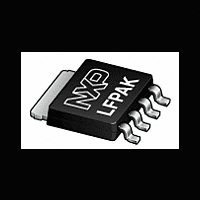
Logic level enhancement mode N-channel MOSFET in LFPAK package
Manufacturer
NXP Semiconductors
Datasheet
1.PSMN2R6-30YLC.pdf
(15 pages)
NXP Semiconductors
Table 7.
PSMN2R6-30YLC
Product data sheet
Symbol
Q
Source-drain diode
V
t
Q
t
t
rr
a
b
Fig 6.
SD
oss
r
(A)
I
100
D
80
60
40
20
0
function of drain-source voltage; typical values
Output characteristics; drain current as a
0
Characteristics
10
Parameter
output charge
source-drain voltage
reverse recovery time
recovered charge
reverse recovery rise time
reverse recovery fall time
0.5
3.5
4.5
…continued
1
1.5
V
N-channel 30 V 2.8mΩ logic level MOSFET in LFPAK using NextPower
GS
All information provided in this document is subject to legal disclaimers.
003a a f 662
(V) =2.4
V
DS
3.0
2.8
2.6
(V)
Conditions
V
T
I
see
I
V
V
dI
see
S
S
j
GS
GS
GS
2
S
= 25 °C
= 25 A; V
= 25 A; dI
Rev. 01 — 2 May 2011
/dt = -100 A/µs; V
Figure 17
Figure 18
= 0 V; V
= 0 V; V
= 0 V; I
GS
S
S
DS
DS
/dt = -100 A/µs;
= 25 A;
Fig 7.
= 0 V; T
= 15 V; f = 1 MHz;
= 15 V
R
(mΩ)
DS on
DS
7.5
2.5
10
5
0
j
of gate-source voltage; typical values
Drain-source on-state resistance as a function
= 15 V;
= 25 °C;
0
4
PSMN2R6-30YLC
Min
-
-
-
-
-
-
8
Typ
17
0.8
33
31
20
13
12
© NXP B.V. 2011. All rights reserved.
003a a f 663
V
GS
Max
-
1.1
-
-
-
-
(V)
16
Unit
nC
V
ns
nC
ns
ns
7 of 15


