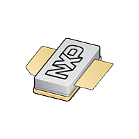
BLF7G15LS-200 NXP Semiconductors, BLF7G15LS-200 Datasheet

BLF7G15LS-200
Available stocks
Related parts for BLF7G15LS-200
BLF7G15LS-200 Summary of contents
Page 1
... BLF7G15LS-200 Power LDMOS transistor Rev. 3 — 22 July 2011 1. Product profile 1.1 General description 200 W LDMOS power transistor for base station applications at frequencies from 1450 MHz to 1550 MHz. Table 1. Typical RF performance at T Mode of operation 2-carrier W-CDMA [1] Test signal: 3GPP; test model 1; 64 DPCH; PAR = 7 0.01 % probability on CCDF per carrier. ...
Page 2
... Parameter thermal resistance from junction to case Characteristics C unless otherwise specified. drain-source breakdown voltage V gate-source threshold voltage drain leakage current All information provided in this document is subject to legal disclaimers. Rev. 3 — 22 July 2011 BLF7G15LS-200 Power LDMOS transistor Simplified outline Symbol Conditions = 80 ...
Page 3
... Mode of operation: 1-carrier W-CDMA; PAR = 7 0.01 % probability on the CCDF; 3GPP test model 1; 64 DPCH; f unless otherwise specified class-AB production test circuit. Symbol PAR O 7.1 Ruggedness in class-AB operation The BLF7G15LS-200 is capable of withstanding a load mismatch corresponding to VSWR = through all phases under the following conditions 1600 mA 7.2 Impedance information Table 9. ...
Page 4
... 1600 mA 1511 MHz One-tone CW power gain and drain efficiency as function of load power; typical values All information provided in this document is subject to legal disclaimers. Rev. 3 — 22 July 2011 BLF7G15LS-200 Power LDMOS transistor drain Z L 001aaf059 014aab253 60 (1) η ...
Page 5
... P (W) L Fig 6. All information provided in this document is subject to legal disclaimers. Rev. 3 — 22 July 2011 BLF7G15LS-200 Power LDMOS transistor 0 (1) (2) ( 100 P L(AV 1600 mA 1511 MHz tone spacing 0.1 MHz. Two-tone intermodulation distortion as a function of average load power ...
Page 6
... All information provided in this document is subject to legal disclaimers. Rev. 3 — 22 July 2011 BLF7G15LS-200 Power LDMOS transistor − + C11 C5 (1) BLF7G15L-200 C10 ...
Page 7
... REFERENCES JEDEC JEITA All information provided in this document is subject to legal disclaimers. Rev. 3 — 22 July 2011 BLF7G15LS-200 Power LDMOS transistor 1.70 20.70 9.91 0.25 1.45 20.45 9.65 0.067 0.815 0.390 0.010 ...
Page 8
... The status of this data sheet has been changed to Product data sheet 20110301 Preliminary data sheet 20100913 Preliminary data sheet All information provided in this document is subject to legal disclaimers. Rev. 3 — 22 July 2011 BLF7G15LS-200 Power LDMOS transistor Change notice Supersedes - BLF7G15LS-200 v.2 - BLF7G15LS-200 v © NXP B.V. 2011. All rights reserved ...
Page 9
... Export control — This document as well as the item(s) described herein may be subject to export control regulations. Export might require a prior authorization from national authorities. All information provided in this document is subject to legal disclaimers. Rev. 3 — 22 July 2011 BLF7G15LS-200 Power LDMOS transistor © NXP B.V. 2011. All rights reserved ...
Page 10
... Notice: All referenced brands, product names, service names and trademarks are the property of their respective owners. http://www.nxp.com salesaddresses@nxp.com All information provided in this document is subject to legal disclaimers. Rev. 3 — 22 July 2011 BLF7G15LS-200 Power LDMOS transistor © NXP B.V. 2011. All rights reserved ...
Page 11
... Please be aware that important notices concerning this document and the product(s) described herein, have been included in section ‘Legal information’. © NXP B.V. 2011. For more information, please visit: http://www.nxp.com For sales office addresses, please send an email to: salesaddresses@nxp.com All rights reserved. Date of release: 22 July 2011 Document identifier: BLF7G15LS-200 ...


