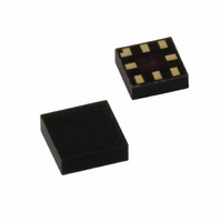
NC7SP74L8X Fairchild Semiconductor, NC7SP74L8X Datasheet - Page 2

NC7SP74L8X
Manufacturer Part Number
NC7SP74L8X
Description
IC FLIP FLOP ULP D 8-MICROPAK
Manufacturer
Fairchild Semiconductor
Series
7SPr
Type
D-Typer
Datasheet
1.NC7SP74L8X.pdf
(12 pages)
Specifications of NC7SP74L8X
Function
Set(Preset) and Reset
Output Type
Differential
Number Of Elements
1
Number Of Bits Per Element
1
Frequency - Clock
40MHz
Delay Time - Propagation
24ns
Trigger Type
Positive Edge
Current - Output High, Low
2.6mA, 2.6mA
Voltage - Supply
0.9 V ~ 3.6 V
Operating Temperature
-40°C ~ 85°C
Mounting Type
Surface Mount
Package / Case
8-MicroPak™
Number Of Circuits
1
Logic Family
7S
Logic Type
D-Type Flip-Flop
Polarity
Inverting/Non-Inverting
Input Type
Single-Ended
Propagation Delay Time
27 ns
High Level Output Current
- 2.6 mA
Low Level Output Current
2.6 mA
Supply Voltage (max)
3.6 V
Maximum Operating Temperature
+ 85 C
Mounting Style
SMD/SMT
Minimum Operating Temperature
- 40 C
Supply Voltage (min)
0.9 V
Lead Free Status / RoHS Status
Lead free / RoHS Compliant
www.fairchildsemi.com
Pin Descriptions
Truth Table
H
L
Q
X
Z
CLR
n
H
H
H
H
LOW Logic Level
L
L
High Impedance
Rising Edge
Falling edge
HIGH Logic Level
Immaterial
No change in data
Pin Names
Q, Q
CLR
CK
PR
D
PR
H
H
H
H
L
L
Inputs
D
X
X
X
H
X
L
CK
X
X
X
Direct Preset Input
Clock Pulse Input
Direct Clear Input
Flip-Flop Output
Q
Q
H
H
H
L
L
Description
Outputs
Data Input
n
Q
Q
H
H
H
L
L
n
No Change
Function
Preset
Clear
—
—
—
2
Logic Symbol
Connection Diagrams
AAA represents Product Code Top Mark - see ordering code
Note: Orientation of Top Mark determines Pin One location. Read the top
product code mark left to right, Pin One is the lower left pin (see diagram).
Pad Assignments for MicroPak
Pin One Orientation Diagram
Pin Assignments for US8
(Top Thru View)
(Top View)
IEEE/IEC


