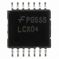
74LCX04MTCX Fairchild Semiconductor, 74LCX04MTCX Datasheet - Page 3

74LCX04MTCX
Manufacturer Part Number
74LCX04MTCX
Description
IC INVERTER HEX 5VINPUT 14TSSOP
Manufacturer
Fairchild Semiconductor
Series
74LCXr
Datasheet
1.74LCX04MTCX.pdf
(13 pages)
Specifications of 74LCX04MTCX
Logic Type
Inverter
Number Of Inputs
1
Number Of Circuits
6
Current - Output High, Low
24mA, 24mA
Voltage - Supply
2 V ~ 3.6 V
Operating Temperature
-40°C ~ 85°C
Mounting Type
Surface Mount
Package / Case
14-TSSOP
Logic Family
74LCX
High Level Output Current
- 24 mA
Low Level Output Current
24 mA
Supply Voltage (max)
3.6 V
Supply Voltage (min)
2 V
Maximum Operating Temperature
+ 85 C
Mounting Style
SMD/SMT
Operating Supply Voltage
2 V to 3.6 V
Output Current
24mA
No. Of Inputs
1
Supply Voltage Range
2V To 3.6V
Logic Case Style
TSSOP
No. Of Pins
14
Operating Temperature Range
-40°C To +85°C
Filter Terminals
SMD
Rohs Compliant
Yes
Family Type
LCX
Lead Free Status / RoHS Status
Lead free / RoHS Compliant
Other names
74LCX04MTCXTR
Available stocks
Company
Part Number
Manufacturer
Quantity
Price
Company:
Part Number:
74LCX04MTCX
Manufacturer:
FAIRCHIL
Quantity:
5 000
Part Number:
74LCX04MTCX
Manufacturer:
FAIRCHILD/仙童
Quantity:
20 000
©1995 Fairchild Semiconductor Corporation
74LCX04 Rev. 1.6.0
Absolute Maximum Ratings
Stresses exceeding the absolute maximum ratings may damage the device. The device may not function or be
operable above the recommended operating conditions and stressing the parts to these levels is not recommended.
In addition, extended exposure to stresses above the recommended operating conditions may affect device reliability.
The absolute maximum ratings are stress ratings only.
Note:
2. I
Recommended Operating Conditions
The Recommended Operating Conditions table defines the conditions for actual device operation. Recommended
operating conditions are specified to ensure optimal performance to the datasheet specifications. Fairchild does not
recommend exceeding them or designing to absolute maximum ratings.
Note:
3. Unused inputs must be held HIGH or LOW. They may not float.
Symbol
Symbol
I
O
OH
T
I
V
V
t / V
I
GND
I
Absolute Maximum Rating must be observed.
V
V
I
STG
T
V
OK
I
CC
V
CC
IK
CC
O
/ I
O
O
A
I
I
OL
Supply Voltage
DC Input Voltage
DC Output Voltage, Output in HIGH or LOW State
DC Input Diode Current, V
DC Output Diode Current
DC Output Source/Sink Current
DC Supply Current per Supply Pin
DC Ground Current per Ground Pin
Storage Temperature
Supply Voltage
Input Voltage
Output Voltage, HIGH or LOW State
Output Current
Free-Air Operating Temperature
Input Edge Rate, V
V
V
Operating
Data Retention
V
V
V
O
O
CC
CC
CC
V
GND
CC
3.0V–3.6V
2.7V–3.0V
2.3V–2.7V
IN
0.8V–2.0V, V
Parameter
I
GND
Parameter
CC
(3)
3.0V
3
(2)
Min.
–40
2.0
1.5
0
0
0
Max.
V
±24
±12
3.6
3.6
5.5
–0.5V to V
±8
85
10
CC
Rating
–65°C to +150°C
–0.5V to +7.0V
–0.5V to +7.0V
www.fairchildsemi.com
CC
±100mA
±100mA
Units
ns / V
–50mA
–50mA
+50mA
±50mA
mA
°C
+ 0.5V
V
V
V


