MM74HCT138M Fairchild Semiconductor, MM74HCT138M Datasheet - Page 3
MM74HCT138M
Manufacturer Part Number
MM74HCT138M
Description
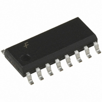
IC DECODER 3-TO-8 LINE 16-SOIC
Manufacturer
Fairchild Semiconductor
Series
74HCTr
Type
Decoderr
Datasheet
1.MM74HCT138N.pdf
(7 pages)
Specifications of MM74HCT138M
Circuit
1 x 3:8
Independent Circuits
1
Current - Output High, Low
4.8mA, 4.8mA
Voltage Supply Source
Single Supply
Voltage - Supply
4.5 V ~ 5.5 V
Operating Temperature
-40°C ~ 85°C
Mounting Type
Surface Mount
Package / Case
16-SOIC (3.9mm Width)
Product
Decoders, Encoders, Multiplexers & Demultiplexers
Logic Family
74HCT
Number Of Lines (input / Output)
3.0 / 8.0
Supply Voltage (max)
5.5 V
Supply Voltage (min)
4.5 V
Maximum Operating Temperature
+ 85 C
Minimum Operating Temperature
- 40 C
Mounting Style
SMD/SMT
Number Of Input Lines
3.0
Number Of Output Lines
8.0
Power Dissipation
600 mW
Logic Type
Decoder
No. Of Outputs
8
Supply Voltage Range
4.5V To 5.5V
Logic Case Style
SOIC
No. Of Pins
16
Operating Temperature Range
-40°C To +85°C
Filter Terminals
SMD
Rohs Compliant
Yes
Logical Function
Decoder/Demux
Number Of Elements
1
Polarity
Inverting
Number Of Inputs
3
Number Of Outputs
8
Output Type
Standard
Propagation Delay Time
50ns
Package Type
SOIC N
High Level Output Current
-4.8mA
Low Level Output Current
4.8mA
Operating Supply Voltage (typ)
5V
Operating Supply Voltage (max)
5.5V
Operating Supply Voltage (min)
4.5V
Operating Temp Range
-40C to 85C
Operating Temperature Classification
Industrial
Mounting
Surface Mount
Pin Count
16
Quiescent Current
8uA
Technology
CMOS
Family Type
HCT
Applications
Memory Address Decoding, Data Routing
Lead Free Status / RoHS Status
Lead free / RoHS Compliant
Available stocks
Company
Part Number
Manufacturer
Quantity
Price
Company:

Part Number:
MM74HCT138MX
Manufacturer:
FSC
Quantity:
2 500


V
V
V
V
I
I
Symbol
IN
CC
Absolute Maximum Ratings
(Note 3)
DC Electrical Characteristics
V
IH
IL
OH
OL
Note 5: This is measured per input pin. All other inputs are held at V
Supply Voltage (V
DC Input Voltage (V
DC Output Voltage (V
Clamp Diode Current (I
DC Output Current, per pin (I
DC V
Storage Temperature Range (T
Power Dissipation (P
Lead Temperature (T
CC
(Note 4)
S.O. Package only
(Soldering 10 seconds)
5V 10% (unless otherwise specified)
CC
Minimum HIGH Level
Input Voltage
Maximum LOW Level
Input Voltage
Minimum HIGH Level
Output Voltage
Maximum LOW Level
Voltage
Maximum Input
Current
Maximum Quiescent
Supply Current
or GND Current, per pin (I
Parameter
CC
IN
)
D
L
OUT
)
)
)
IK
, I
)
OK
OUT
)
STG
)
CC
)
V
|I
|I
|I
V
|I
|I
|I
V
V
V
I
V
)
OUT
OUT
OUT
OUT
OUT
OUT
OUT
IN
IN
IN
IH
IN
IN
or V
|
|
|
|
|
|
V
V
V
V
2.4V or 0.5V (Note 5)
1.5 to V
0.5 to V
0 A
IH
IH
CC
CC
65 C to 150 C
20 A
4.0 mA, V
4.8 mA, V
20 A
4.0 mA, V
4.8 mA, V
IL
or V
or V
Conditions
or GND,
or GND
(Note 2)
0.5 to 7.0V
IL
IL
CC
CC
600 mW
500 mW
CC
CC
CC
CC
20 mA
25 mA
50 mA
CC
260 C
1.5V
0.5V
or ground.
4.5V
5.5V
4.5V
5.5V
3
Recommended Operating
Conditions
Note 2: Absolute Maximum Ratings are those values beyond which dam-
age to the device may occur.
Note 3: Unless otherwise specified all voltages are referenced to ground.
Note 4: Power Dissipation temperature derating — plastic “N” package:
12 mW/ C from 65 C to 85 C.
Supply Voltage (V
DC Input or Output Voltage
Operating Temperature Range (T
Input Rise or Fall Times
(V
(t
r
, t
IN
Typ
V
4.2
5.2
0.2
0.2
CC
0
f
, V
)
T
A
OUT
25 C
V
)
CC
3.98
4.98
0.26
0.26
2.0
0.8
0.1
8.0
0.3
0.1
0.1
CC
)
T
A
Guaranteed Limits
V
CC
40 to 85 C T
3.84
4.84
0.33
0.33
2.0
0.8
0.1
0.4
80
1.0
0.1
A
)
Min
4.5
A
40
0
www.fairchildsemi.com
V
CC
55 to 125 C
160
2.0
0.8
3.7
4.7
0.1
0.4
0.4
0.5
1.0
Max
V
500
5.5
0.1
CC
85
Units
ns
V
V
C
Units
mA
V
V
V
V
V
V
V
V
A
A
Related parts for MM74HCT138M
Image
Part Number
Description
Manufacturer
Datasheet
Request
R

Part Number:
Description:
Fairchild Semiconductor [IGBT MODULE]
Manufacturer:
Fairchild Semiconductor
Datasheet:

Part Number:
Description:
Discrete Semiconductor Modules
Manufacturer:
Fairchild Semiconductor
Part Number:
Description:
Discrete Semiconductor Modules
Manufacturer:
Fairchild Semiconductor
Part Number:
Description:
This N-Channel MOSFET is produced using Fairchild Semiconductor’s advanced Power Trench® process
Manufacturer:
Fairchild Semiconductor
Datasheet:
Part Number:
Description:
This N-Channel MOSFET is produced using Fairchild Semiconductor’s advanced Power Trench® process
Manufacturer:
Fairchild Semiconductor
Datasheet:
Part Number:
Description:
This N-Channel MOSFET is produced using Fairchild Semiconductor’s advanced PowerTrench® process
Manufacturer:
Fairchild Semiconductor
Datasheet:
Part Number:
Description:
This N-Channel MOSFET is produced using Fairchild Semiconductor’s advanced PowerTrench® process
Manufacturer:
Fairchild Semiconductor
Datasheet:
Part Number:
Description:
This N-Channel MOSFET is produced using Fairchild Semiconductor’s advanced Power Trench® process
Manufacturer:
Fairchild Semiconductor
Datasheet:
Part Number:
Description:
This N-Channel logic Level MOSFETs are produced using Fairchild Semiconductor‘s advanced Power Trench® process that has been special tailored to minimize the on-state resistance and yet maintain superior switching performance
Manufacturer:
Fairchild Semiconductor
Datasheet:
Part Number:
Description:
This N-Channel MOSFET is produced using Fairchild Semiconductor’s advanced Power Trench® process
Manufacturer:
Fairchild Semiconductor
Datasheet:
Part Number:
Description:
This N-Channel SyncFET™ is produced using Fairchild Semiconductor’s advanced PowerTrench® process
Manufacturer:
Fairchild Semiconductor
Datasheet:
Part Number:
Description:
This N-Channel SyncFET™ is produced using Fairchild Semiconductor’s advanced PowerTrench® process
Manufacturer:
Fairchild Semiconductor
Datasheet:
Part Number:
Description:
This N-Channel SyncFET™ is produced using Fairchild Semiconductor’s advanced PowerTrench® process
Manufacturer:
Fairchild Semiconductor
Datasheet: