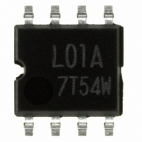
BR24L01AF-WE2 Rohm Semiconductor, BR24L01AF-WE2 Datasheet - Page 14

BR24L01AF-WE2
Manufacturer Part Number
BR24L01AF-WE2
Description
IC EEPROM 1KBIT 400KHZ 8SOP
Manufacturer
Rohm Semiconductor
Specifications of BR24L01AF-WE2
Memory Size
1K (128 x 8)
Format - Memory
EEPROMs - Serial
Memory Type
EEPROM
Speed
400kHz
Interface
I²C, 2-Wire Serial
Voltage - Supply
1.8 V ~ 5.5 V
Operating Temperature
-40°C ~ 85°C
Package / Case
8-SOP
Clock Frequency
400kHz
Supply Voltage Range
1.8V To 5.5V
Memory Case Style
SOP
No. Of Pins
8
Operating Temperature Range
-40°C To +85°C
Svhc
No SVHC (18-Jun-2010)
Package /
RoHS Compliant
Memory Configuration
128 X 8
Interface Type
I2C, Serial
Rohs Compliant
Yes
Lead Free Status / RoHS Status
Lead free / RoHS Compliant
Other names
BR24L01AF-WE2TR
Available stocks
Company
Part Number
Manufacturer
Quantity
Price
Company:
Part Number:
BR24L01AF-WE2
Manufacturer:
ROHM Semiconductor
Quantity:
1 835
Company:
Part Number:
BR24L01AF-WE2
Manufacturer:
ROHM
Quantity:
21 523
Part Number:
BR24L01AF-WE2
Manufacturer:
ROHM/罗姆
Quantity:
20 000
●Software reset
●Acknowledge polling
© 2009 ROHM Co., Ltd. All rights reserved.
BR24L□□-W Series,BR24S□□□-W Series
www.rohm.com
Software reset is executed when to avoid malfunction after power on, and to reset during command input. Software reset
has several kinds, and 3 kinds of them are shown in the figure below. (Refer to Fig.48(a), Fig.48(b), and Fig.48(c).) In
dummy clock input area, release the SDA bus ('H' by pull up). In dummy clock area, ACK output and read data '0' (both 'L'
level) may be output from EEPROM, therefore, if 'H' is input forcibly, output may conflict and over current may flow, leading
to instantaneous power failure of system power source or influence upon devices.
During internal write execution, all input commands are ignored, therefore ACK is not sent back. During internal automatic
write execution after write cycle input, next command (slave address) is sent, and if the first ACK signal sends back 'L', then
it means end of write action, while if it sends back 'H', it means now in writing. By use of acknowledge polling, next command
can be executed without waiting for tWR = 5ms.
When to write continuously, R/W = 0, when to carry out current read cycle after write, slave address R/W = 1 is sent, and if
ACK signal sends back 'L', then execute word address input and data output and so forth.
SCL
SDA
SCL
SDA
SDA
SCL
…
Fig.48-(b) The case of START +9 dummy clocks +START+ command input
S
T
A
R
T
Fig.48-(a) The case of dummy clock +START+START+ command input
First write command
S
T
A
R
T
Write command
Slave
address
t
Fig.49 Case to continuously write by acknowledge polling
WR
Start
1
1
A
C
K
H
Fig.48-(c) START×9+ command input
Dummy clock×14
2
1
S
T
O
P
2
Dummy clock×9
S
T
A
R
T
2
3
Slave
address
S
T
A
R
T
Start×9
Slave
address
13
14/40
Second write command
A
C
K
L
14
8
7
After completion of internal write,
ACK=LOW is sent back, so input next
word address and data in succession.
A
C
K
H
Word
address
t
WR
9
Start×2
8
During internal write,
ACK = HIGH is sent back.
S
T
A
R
T
Start
Slave
address
A
C
K
L
9
* Start command from START input.
Data
A
C
K
H
A
C
K
L
S
T
O
P
Normal command
Normal command
Normal command
Normal command
Normal command
Normal command
Technical Note
2009.09 - Rev.D


