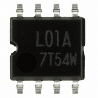
BR24L01AF-WE2 Rohm Semiconductor, BR24L01AF-WE2 Datasheet - Page 5

BR24L01AF-WE2
Manufacturer Part Number
BR24L01AF-WE2
Description
IC EEPROM 1KBIT 400KHZ 8SOP
Manufacturer
Rohm Semiconductor
Specifications of BR24L01AF-WE2
Memory Size
1K (128 x 8)
Format - Memory
EEPROMs - Serial
Memory Type
EEPROM
Speed
400kHz
Interface
I²C, 2-Wire Serial
Voltage - Supply
1.8 V ~ 5.5 V
Operating Temperature
-40°C ~ 85°C
Package / Case
8-SOP
Clock Frequency
400kHz
Supply Voltage Range
1.8V To 5.5V
Memory Case Style
SOP
No. Of Pins
8
Operating Temperature Range
-40°C To +85°C
Svhc
No SVHC (18-Jun-2010)
Package /
RoHS Compliant
Memory Configuration
128 X 8
Interface Type
I2C, Serial
Rohs Compliant
Yes
Lead Free Status / RoHS Status
Lead free / RoHS Compliant
Other names
BR24L01AF-WE2TR
Available stocks
Company
Part Number
Manufacturer
Quantity
Price
Company:
Part Number:
BR24L01AF-WE2
Manufacturer:
ROHM Semiconductor
Quantity:
1 835
Company:
Part Number:
BR24L01AF-WE2
Manufacturer:
ROHM
Quantity:
21 523
Part Number:
BR24L01AF-WE2
Manufacturer:
ROHM/罗姆
Quantity:
20 000
●Sync data input / output timing
© 2009 ROHM Co., Ltd. All rights reserved.
BR24L□□-W Series,BR24S□□□-W Series
www.rohm.com
○Input read at the rise edge of SCL
○Data output in sync with the fall of SCL
○At write execution, in the area from the D0 taken clock rise of the first
○By setting WP “HIGH” in the area, write can be cancelled.
SDA
SCL
SCL
SDA
DATA(1), to tWR, set WP=“LOW”.
(output)
WP
When it is set WP=“HIGH” during tWR, write is forcibly ended, and data
of address under access is not guaranteed, therefore write it once again.
(input)
SCL
SDA
(入力)
SDA
(出力)
(n-th address)
D1
Fig.1-(a) Sync data input / output timing
Write data
tHD:STA
DATA(1)
tBUF
Fig.1-(e) WP timing at write cance
D0
D0
Fig.1-(c) Write cycle timing
ACK
ACK
tR
tSU:DAT
tHIGH:WP
Stop condition
DATA(n)
tPD
tF
tLOW
tW R
tHIGH
Start condition
ACK
tDH
tHD:DAT
tWR
5/40
SCL
SDA
WP
SCL
SDA
D1
DATA(1)
tSU:WP
Fig.1-(d) WP timing at write execution
tSU:STA
D0
Fig.1-(b) Start-stop bit timing
ACK
tHD:STA
START BIT
DATA(n)
tSU:STO
ACK
ストップコンディション
Stop condition
Technical Note
2009.09 - Rev.D
tWR
STOP BIT
tHD:WP


