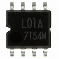
BR24L01AF-WE2 Rohm Semiconductor, BR24L01AF-WE2 Datasheet - Page 6

BR24L01AF-WE2
Manufacturer Part Number
BR24L01AF-WE2
Description
IC EEPROM 1KBIT 400KHZ 8SOP
Manufacturer
Rohm Semiconductor
Specifications of BR24L01AF-WE2
Memory Size
1K (128 x 8)
Format - Memory
EEPROMs - Serial
Memory Type
EEPROM
Speed
400kHz
Interface
I²C, 2-Wire Serial
Voltage - Supply
1.8 V ~ 5.5 V
Operating Temperature
-40°C ~ 85°C
Package / Case
8-SOP
Clock Frequency
400kHz
Supply Voltage Range
1.8V To 5.5V
Memory Case Style
SOP
No. Of Pins
8
Operating Temperature Range
-40°C To +85°C
Svhc
No SVHC (18-Jun-2010)
Package /
RoHS Compliant
Memory Configuration
128 X 8
Interface Type
I2C, Serial
Rohs Compliant
Yes
Lead Free Status / RoHS Status
Lead free / RoHS Compliant
Other names
BR24L01AF-WE2TR
Available stocks
Company
Part Number
Manufacturer
Quantity
Price
Company:
Part Number:
BR24L01AF-WE2
Manufacturer:
ROHM Semiconductor
Quantity:
1 835
Company:
Part Number:
BR24L01AF-WE2
Manufacturer:
ROHM
Quantity:
21 523
Part Number:
BR24L01AF-WE2
Manufacturer:
ROHM/罗姆
Quantity:
20 000
●Block diagram
●Pin assignment and description
© 2009 ROHM Co., Ltd. All rights reserved.
BR24L□□-W Series,BR24S□□□-W Series
www.rohm.com
Terminal
name
GND
SDA
SCL
WP
Vcc
A0
A1
A2
GND
*2
*2
*2
A2
A1
A0
Input /
output
Input /
output
Input
Input
Input
Input
Input
1
2
3
4
-
-
*
1 7bit : BR24L01A-W
8bit : BR24L02-W
9bit : BR24L04-W
generating circuit
BR24L01A-W
High voltage
Slave address setting
7bit
8bit
9bit
10bi
Address
decoder
t
*1
11bit
12bit
13b
Slave address setting
it
10bit : BR24L08-W
11bit : BR24L16-W
12bit : BR24L32-W
13bit : BR24L64-W
Control circuit
*1
BR24L02-W
Slave address setting
7bit
8bit
9bit
10bi
Slave and word address, Serial data input serial data output
t
11bit
12bit
13b
START
GND
1Kbit~64Kbit EEPROM array
Fig.2 Block diagram
it
A0
A1
A2
voltage detection
Power source
Reference voltage of all input / output, 0V
1
2
3
4
Slave - word
address register
1
1
1
1
BR24L04-W
6/40
BR24L01A-W
BR24L02-W
BR24L04-W
BR24L08-W
BR24L16-W
BR24L32-W
BR24L64-W
STOP
Connect the power source.
*
2 A0=N.C.
Write protect terminal
A0, A1=N.C.
A0, A1= N.C. A2=Don’t Use
Serial clock input
Not connected
BR24L08-W
Function
8
7
5
6
1
1
1
1
ACK
Vcc
WP
SCL
SDA
Not connected
register
Data
8bit
BR24L16-W
Not used
: BR24L16-W
: BR24L04-W
: BR24L08-W
8
7
6
5
BR24L32-W
Slave address setting
Slave address setting
Slave address setting
Vcc
WP
SCL
SDA
Technical Note
2009.09 - Rev.D
BR24L64-W


