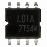
BR24L01AF-WE2 Rohm Semiconductor, BR24L01AF-WE2 Datasheet - Page 36

BR24L01AF-WE2
Manufacturer Part Number
BR24L01AF-WE2
Description
IC EEPROM 1KBIT 400KHZ 8SOP
Manufacturer
Rohm Semiconductor
Specifications of BR24L01AF-WE2
Memory Size
1K (128 x 8)
Format - Memory
EEPROMs - Serial
Memory Type
EEPROM
Speed
400kHz
Interface
I²C, 2-Wire Serial
Voltage - Supply
1.8 V ~ 5.5 V
Operating Temperature
-40°C ~ 85°C
Package / Case
8-SOP
Clock Frequency
400kHz
Supply Voltage Range
1.8V To 5.5V
Memory Case Style
SOP
No. Of Pins
8
Operating Temperature Range
-40°C To +85°C
Svhc
No SVHC (18-Jun-2010)
Package /
RoHS Compliant
Memory Configuration
128 X 8
Interface Type
I2C, Serial
Rohs Compliant
Yes
Lead Free Status / RoHS Status
Lead free / RoHS Compliant
Other names
BR24L01AF-WE2TR
Available stocks
Company
Part Number
Manufacturer
Quantity
Price
Company:
Part Number:
BR24L01AF-WE2
Manufacturer:
ROHM Semiconductor
Quantity:
1 835
Company:
Part Number:
BR24L01AF-WE2
Manufacturer:
ROHM
Quantity:
21 523
Part Number:
BR24L01AF-WE2
Manufacturer:
ROHM/罗姆
Quantity:
20 000
●I
●Notes on power ON
© 2009 ROHM Co., Ltd. All rights reserved.
BR24L□□-W Series,BR24S□□□-W Series
www.rohm.com
2
○Input (A0, A1, A2, SCL, WP)
○Input/Output (SDA)
At power on, in IC internal circuit and set, Vcc rises through unstable low voltage area, and IC inside is not completely reset,
and malfunction may occur. To prevent this, functions of POR circuit and LVCC circuit are equipped. To assure the action,
observe the following condition at power on.
C BUS input / output circuit
1. Set SDA = 'H' and SCL ='L' or 'H'
2. Start power source so as to satisfy the recommended conditions of tR, tOFF, and Vbot for operating POR circuit.
3. Set SDA and SCL so as not to become 'Hi-Z'.
When the above conditions 1 and 2 cannot be observed, take the following countermeasures.
a) In the case when the above conditions 1 cannot be observed. When SDA becomes 'L' at power on .
b) In the case when the above condition 2 cannot be observed.
c) In the case when the above conditions 1 and 2 cannot be observed.
→Control SCL and SDA as shown below, to make SCL and SDA, 'H' and 'H'.
→After power source becomes stable, execute software reset(P26).
→Carry out a), and then carry out b).
SCL
SDA
V
CC
After Vcc becomes stable
V
CC
0
Fig.57 When SCL='H' and SDA='L'
Fig.56 Rise waveform diagram
Fig.54 Input pin circuit diagram
Fig.55 Input /output pin circuit diagram
tOFF
tDH
tLOW
tR
tSU:DAT
Vbot
36/40
Recommended conditions of tR,tOFF,Vbot
100ms or below
10ms or below
tR
After Vcc becomes stable
Fig.58 When SCL='H' and SDA='L'
10ms or longer
10ms or longer
tOFF
tSU:DAT
Technical Note
2009.09 - Rev.D
0.3V or below
0.2V or below
Vbot


