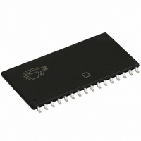
CY62148EV30LL-45ZSXI Cypress Semiconductor Corp, CY62148EV30LL-45ZSXI Datasheet - Page 4

CY62148EV30LL-45ZSXI
Manufacturer Part Number
CY62148EV30LL-45ZSXI
Description
IC SRAM 4MBIT 45NS 32TSOP
Manufacturer
Cypress Semiconductor Corp
Type
Asynchronousr
Datasheet
1.CY62148EV30LL-45BVXI.pdf
(15 pages)
Specifications of CY62148EV30LL-45ZSXI
Memory Size
4M (512K x 8)
Package / Case
32-TSOP II
Format - Memory
RAM
Memory Type
SRAM
Speed
45ns
Interface
Parallel
Voltage - Supply
2.2 V ~ 3.6 V
Operating Temperature
-40°C ~ 85°C
Access Time
45 ns
Supply Voltage (max)
3.6 V
Supply Voltage (min)
2.2 V
Maximum Operating Current
20 mA
Organization
512 K x 8
Maximum Operating Temperature
+ 85 C
Minimum Operating Temperature
- 40 C
Mounting Style
SMD/SMT
Number Of Ports
1
Operating Supply Voltage
3 V
Memory Configuration
512K X 8
Supply Voltage Range
2.2V To 3.6V
Memory Case Style
TSOP
No. Of Pins
44
Operating Temperature Range
-40°C To +85°C
Rohs Compliant
Yes
Density
4Mb
Access Time (max)
45ns
Sync/async
Asynchronous
Architecture
Not Required
Clock Freq (max)
Not RequiredMHz
Operating Supply Voltage (typ)
2.5/3.3V
Address Bus
19b
Package Type
TSOP-II
Operating Temp Range
-40C to 85C
Supply Current
20mA
Operating Supply Voltage (min)
2.2V
Operating Supply Voltage (max)
3.6V
Operating Temperature Classification
Industrial
Mounting
Surface Mount
Pin Count
32
Word Size
8b
Number Of Words
512K
Lead Free Status / RoHS Status
Lead free / RoHS Compliant
Lead Free Status / RoHS Status
Lead free / RoHS Compliant, Lead free / RoHS Compliant
Other names
428-2076
CY62148EV30LL-45ZSXI
CY62148EV30LL-45ZSXI
Available stocks
Company
Part Number
Manufacturer
Quantity
Price
Company:
Part Number:
CY62148EV30LL-45ZSXI
Manufacturer:
CYPRESS
Quantity:
117 000
Part Number:
CY62148EV30LL-45ZSXI
Manufacturer:
CYPRESS/赛普拉斯
Quantity:
20 000
Company:
Part Number:
CY62148EV30LL-45ZSXIT
Manufacturer:
TI
Quantity:
15
Company:
Part Number:
CY62148EV30LL-45ZSXIT
Manufacturer:
CYPRESS
Quantity:
455
Part Number:
CY62148EV30LL-45ZSXIT
Manufacturer:
CYPRESS/赛普拉斯
Quantity:
20 000
Maximum Ratings
Exceeding maximum ratings may impair the useful life of the
device. These user guidelines are not tested.
Storage temperature................................. –65 °C to +150 °C
Ambient temperature with
power applied ............................................. 55 °C to +125 °C
Supply voltage to ground
potential ........................................–0.3 V to V
DC voltage applied to outputs
in High-Z State
Electrical Characteristics
(Over the Operating Range)
Document #: 38-05576 Rev. *K
Notes
V
V
V
V
I
I
I
I
I
Parameter
5. V
6. V
7. Full device AC operation assumes a minimum of 100 s ramp time from 0 to V
8. SOIC package is available only in 55 ns speed bin.
9. Typical values are included for reference only and are not guaranteed or tested. Typical values are measured at V
10. Under DC conditions the device meets a V
11. Only chip enable (CE) must be HIGH at CMOS level to meet the I
IX
OZ
CC
SB1
SB2
OH
OL
IH
IL
LOW voltage applied to the device must not be higher than 0.6V and 0.4V for the above ranges. This is applicable to SOIC package only. Refer to AN13470 for details.
[11]
IL(min)
IH(max)
= –2.0V for pulse durations less than 20 ns.
= V
Output high voltage I
Output low voltage
Input high voltage
Input low voltage
Input leakage
current
Output leakage
current
V
supply current
Automatic CE power
down current —
CMOS inputs
Automatic CE power
down current —
CMOS inputs
CC
CC
+ 0.75V for pulse durations less than 20 ns.
[5, 6]
Description
operating
......................–0.3 V to V
I
I
I
V
V
V
2.7 V
V
3.6 V
GND < V
GND < V
f = f
f = 1 MHz
CE > V
V
f = f
f = 0 (OE and WE), V
CE > V
V
f = 0, V
OH
OH
OL
OL
CC
CC
CC
CC
IN
IN
IL
= 0.1 mA
= 2.1 mA, V
max
> V
max
= –0.1 mA
= –1.0 mA, V
> V
of 0.8V (for V
= 2.7V to 3.6 V
= 2.2V to
= 2.7V to
= 2.2V to 2.7 V
CC
CC
CC
CC
CC
= 1/t
(Address and Data Only),
Test Conditions
I
O
< V
– 0.2V ,
– 0.2V, V
– 0.2 V,
= 3.60 V
– 0.2 V or V
CC(max)
CC(max)
< V
RC
C
CC
CC
CC
For VFBGA and
TSOP II package
For SOIC package
For VFBGA and
TSOP II package
For SOIC package
V
I
CMOS levels
OUT
range of 2.7V to 3.6V) and 0.6V (for V
, Output Disabled
CC
CC
+ 0.3 V
> 2.70 V
+ 0.3 V
IN
> 2.70 V
SB2
= V
= 0 mA,
CC
< 0.2 V
IN
/ I
CC(max),
= 3.60 V
CCDR
< 0.2 V,
spec. Other inputs can be left floating.
CC(min)
DC input voltage
Output current into outputs (LOW) .............................. 20 mA
Static discharge voltage.......................................... > 2001 V
(MIL-STD-883, Method 3015)
Latch up current...................................................... > 200 mA
Operating Range
CY62148EV30
–0.3
–0.3
and 200 s wait time after V
Min
2.0
2.4
1.8
2.2
–45 (Industrial/Auto-A)
–1
–1
Product
Typ
15
2
1
1
CC
[9]
range of 2.2V to 2.7V). However, in dynamic conditions Input
V
V
[5, 6]
CC
CC
Industrial/
Max
Range
Auto-A
0.4
0.4
0.6
0.8
2.5
....................–0.3 V to V
+1
+ 0.3 V
+ 0.3 V
+1
20
7
7
CC
CC
stabilization.
= V
CY62148EV30 MoBL
CC(typ)
–0.3
–0.3
Min Typ
2.0
2.4
1.8
2.2
–1
–1
–40°C to +85°C 2.2V to 3.6V
Temperature
, T
Ambient
A
= 25°C.
15
2
1
1
–55
[9]
[8]
V
V
CC(max)
CC
CC
0.4
0.6
Max
0.2
0.4
2.5
+ 0.3 V
+ 0.3 V
+1
+1
20
7
7
[10]
[10]
Page 4 of 15
V
+ 0.3 V
CC
[7]
Unit
mA
A
A
A
A
V
V
V
V
V
V
V
V
V
®
[+] Feedback


