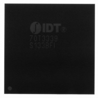
IDT70T3339S133BFI IDT, Integrated Device Technology Inc, IDT70T3339S133BFI Datasheet - Page 14

IDT70T3339S133BFI
Manufacturer Part Number
IDT70T3339S133BFI
Description
IC SRAM 9MBIT 133MHZ 208FBGA
Manufacturer
IDT, Integrated Device Technology Inc
Datasheet
1.IDT70T3339S133BFI.pdf
(27 pages)
Specifications of IDT70T3339S133BFI
Format - Memory
RAM
Memory Type
SRAM - Dual Port, Synchronous
Memory Size
9M (512K x 18)
Speed
133MHz
Interface
Parallel
Voltage - Supply
2.4 V ~ 2.6 V
Operating Temperature
-40°C ~ 85°C
Package / Case
208-FBGA
Lead Free Status / RoHS Status
Lead free / RoHS Compliant
Other names
70T3339S133BFI
800-1378
800-1378
Available stocks
Company
Part Number
Manufacturer
Quantity
Price
Company:
Part Number:
IDT70T3339S133BFI
Manufacturer:
IDT
Quantity:
850
Company:
Part Number:
IDT70T3339S133BFI
Manufacturer:
IDT, Integrated Device Technology Inc
Quantity:
10 000
Company:
Part Number:
IDT70T3339S133BFI8
Manufacturer:
IDT, Integrated Device Technology Inc
Quantity:
10 000
Timing Waveform of Left Port Write to Pipelined Right Port Read
NOTES:
1. CE
2. OE = V
3. If t
4. All timing is the same for Left and Right ports. Port "A" may be either Left or Right port. Port "B" is the opposite of Port "A"
Timing Waveform with Port-to-Port Flow-Through Read
NOTES:
1. CE
2. OE = V
3. If t
4. All timing is the same for both left and right ports. Port "A" may be either left or right port. Port "B" is the opposite of Port "A".
IDT70T3339/19/99S
High-Speed 2.5V 512/256/128K x 18 Dual-Port Static RAM
t
will be t
t
be t
CO
CO
ADDRESS
ADDRESS
DATA
CO
CO
0
0
CO
, UB, LB, and ADS = V
+ 2 t
, UB, LB, and ADS = V
+ t
DATA
< minimum specified, then data from Port "B" read is not valid until following Port "B" clock cycle (ie, time from write to valid read on opposite port will be
< minimum specified, then data from Port "B" read is not valid until following Port "B" clock cycle (i.e., time from write to valid read on opposite port will be
ADDRESS
ADDRESS
CYC
+ t
IL
DATA
IL
CO
CLK
CLK
R/W
R/W
OUT"B"
CYC2
DATA
for Port "B", which is being read from. OE = V
for the Right Port, which is being read from. OE = V
CD1
IN"A"
+ t
+ t
"A"
"A"
"B"
"B"
"B"
"A
CLK
R/W
CLK
R/W
).
+ t
CYC2
CD1
"
OUT "B"
IN "A"
CD2
). If t
"A"
"A"
"A"
"B"
"B"
"B"
+ t
). If t
CD2
CO
CO
).
> minimum, then data from Port "B" read is available on first Port "B" clock cycle (i.e., time from write to valid read on opposite port will
IL
IL
> minimum, then data from Port "B" read is available on first Port "B" clock cycle (ie, time from write to valid read on opposite port
t
t
t
VALID
SW
MATC
SD
; CE
; CE
SA
H
t
t
SW
MATC
SA
1
1
t
t
t
, CNTEN, and REPEAT = V
, CNTEN, and REPEAT = V
HA
HD
HW
H
MATCH
t
t
VALID
t
SA
SD
SW
t
t
HW
HA
MATCH
t
t
SA
SW
t
t
t
HW
HA
HD
t
CO
t
DC
(3)
t
t
HW
HA
t
CO
(3)
IH
for Port "A", which is being written to.
t
CD1
IH
IH
IH
.
.
for the Left Port, which is being written to.
MATC
NO
H
6.42
14
t
CD2
VALID
MATCH
NO
MATCH
Industrial and Commercial Temperature Ranges
NO
VALID
MATCH
NO
t
DC
t
CD1
(1,2,4)
t
DC
VALID
5652 drw 09
(1,2,4)
5652 drw 10
,
,


