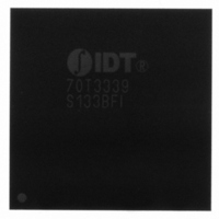
IDT70T3339S133BFI IDT, Integrated Device Technology Inc, IDT70T3339S133BFI Datasheet - Page 8

IDT70T3339S133BFI
Manufacturer Part Number
IDT70T3339S133BFI
Description
IC SRAM 9MBIT 133MHZ 208FBGA
Manufacturer
IDT, Integrated Device Technology Inc
Datasheet
1.IDT70T3339S133BFI.pdf
(27 pages)
Specifications of IDT70T3339S133BFI
Format - Memory
RAM
Memory Type
SRAM - Dual Port, Synchronous
Memory Size
9M (512K x 18)
Speed
133MHz
Interface
Parallel
Voltage - Supply
2.4 V ~ 2.6 V
Operating Temperature
-40°C ~ 85°C
Package / Case
208-FBGA
Lead Free Status / RoHS Status
Lead free / RoHS Compliant
Other names
70T3339S133BFI
800-1378
800-1378
Available stocks
Company
Part Number
Manufacturer
Quantity
Price
Company:
Part Number:
IDT70T3339S133BFI
Manufacturer:
IDT
Quantity:
850
Company:
Part Number:
IDT70T3339S133BFI
Manufacturer:
IDT, Integrated Device Technology Inc
Quantity:
10 000
Company:
Part Number:
IDT70T3339S133BFI8
Manufacturer:
IDT, Integrated Device Technology Inc
Quantity:
10 000
NOTES:
1. Stresses greater than those listed under ABSOLUTE MAXIMUM RATINGS may cause
2. This is a steady-state DC parameter that applies after the power supply has reached its
3. Ambient Temperature under DC Bias. No AC Conditions. Chip Deselected.
Capacitance
(T
NOTES:
1. V
2. Applicable only for TMS, TDI and TRST inputs.
3. Outputs tested in tri-state mode.
NOTES:
1. These parameters are determined by device characterization, but are not
2. 3dV references the interpolated capacitance when the input and output switch
3. C
DC Electrical Characteristics Over the Operating
Temperature and Supply Voltage Range
Absolute Maximum Ratings
V
(V
V
(V
V
(INPUTS and I/O's)
T
T
T
I
I
OUT
OUT
BIAS
STG
JN
IDT70T3339/19/99S
High-Speed 2.5V 512/256/128K x 18 Dual-Port Static RAM
TERM
TERM
TERM
Symbol
V
V
V
V
DD
DDQ
A
permanent damage to the device. This is a stress rating only and functional operation of the
device at these or any other conditions above those indicated in the operational sections
of this specification is not implied. Exposure to absolute maximum rating conditions for
extended periods may affect reliability.
nominal operating value. Power sequencing is not necessary; however, the voltage on
any Input or I/O pin cannot exceed V
C
production tested.
from 0V to 3V or from 3V to 0V.
Symbol
OH
OH
(For V
(For V
OL
OL
)
C
OUT
OUT
DDQ
(3)
= +25°C, f = 1.0MHz) PQFP ONLY
)
|I
(2)
IN
(2)
|I
|I
LO
(3.3V)
(2.5V)
(3.3V)
(2.5V)
Symbol
LI
LI
(3)
|
|
also references C
|
is selectable (3.3V/2.5V) via OPT pins. Refer to p.6 for details.
DDQ
DDQ
Input Capacitance
Output Capacitance
= 3.3V) DC Output Current
= 2.5V) DC Output Current
Input Leakage Current
JTAG & ZZ Input Leakage Current
Output Leakage Current
Output Low Voltage
Output High Voltage
Output Low Voltage
Output High Voltage
Parameter
Input and I/O Terminal
Storage Temperature
Junction Temperature
V
with Respect to GND
V
with Respect to GND
Voltage with Respect to GND
Temperature Under Bias
DD
DDQ
(1)
I/O
Terminal Voltage
.
Terminal Voltage
Parameter
Rating
(1)
(1)
(1)
(1)
(1)
DDQ
(1,3)
during power supply ramp up.
Conditions
V
V
OUT
IN
= 3dV
= 3dV
(1,2)
-0.3 to V
-0.3 to V
(2)
-0.5 to 3.6
Commercial
& Industrial
I
I
I
I
-55 to +125
-65 to +150
V
V
CE
OL
OH
OL
OH
(1)
DDQ
DD =
+150
0
= +4mA, V
= +2mA, V
Max.
= -4mA, V
= -2mA, V
10.5
50
40
DDQ
DDQ
= V
8
= Max., V
Max.
IH
+ 0.3
+ 0.3
5652 tbl 07
or CE
,
Unit
V
pF
pF
IN
DDQ
DDQ
DDQ
DDQ
IN
= 0V to V
1
6.42
= 0V to V
= V
= Min.
= Min.
= Min.
= Min.
8
5652 tbl 06
Unit
mA
mA
o
o
o
V
V
V
C
C
C
IL
Test Conditions
, V
DD
OUT
(V
DDQ
= 0V to V
DD
= 2.5V ± 100mV)
DDQ
Industrial and Commercial Temperature Ranges
Min.
2.4
2.0
70T3339/19/99S
___
___
___
___
___
Max.
±30
0.4
0.4
10
10
___
___
5652 tbl 08
Unit
µ A
µ A
µ A
V
V
V
V


