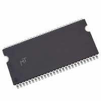
MT48LC8M8A2P-75:G Micron Technology Inc, MT48LC8M8A2P-75:G Datasheet - Page 39

MT48LC8M8A2P-75:G
Manufacturer Part Number
MT48LC8M8A2P-75:G
Description
IC SDRAM 64MBIT 133MHZ 54TSOP
Manufacturer
Micron Technology Inc
Type
SDRAMr
Datasheet
1.MT48LC4M16A2P-75G_TR.pdf
(72 pages)
Specifications of MT48LC8M8A2P-75:G
Format - Memory
RAM
Memory Type
SDRAM
Memory Size
64M (8M x 8)
Speed
133MHz
Interface
Parallel
Voltage - Supply
3 V ~ 3.6 V
Operating Temperature
0°C ~ 70°C
Package / Case
54-TSOP II
Organization
8Mx8
Density
64Mb
Address Bus
14b
Access Time (max)
6/5.4ns
Maximum Clock Rate
133MHz
Operating Supply Voltage (typ)
3.3V
Package Type
TSOP-II
Operating Temp Range
0C to 70C
Operating Supply Voltage (max)
3.6V
Operating Supply Voltage (min)
3V
Supply Current
140mA
Pin Count
54
Mounting
Surface Mount
Operating Temperature Classification
Commercial
Lead Free Status / RoHS Status
Lead free / RoHS Compliant
Figure 32:
Table 8:
PDF: 09005aef80725c0b/Source: 09005aef806fc13c
64MSDRAM_2.fm - Rev. N 12/08 EN
CKE
H
H
L
L
n-1
Truth Table 2 – CKE
Notes 1–4 apply to entire table
WRITE With Auto Precharge Interrupted by a WRITE
CKE
H
H
L
L
Notes:
Notes:
n
1. DQM is LOW.
1. CKE
2. Current state is the state of the SDRAM immediately prior to clock edge n.
3. COMMAND
4. All states and sequences not shown are illegal or reserved.
5. Exiting power-down at clock edge n will put the device in the all banks idle state in time for
6. Exiting self refresh at clock edge n will put the device in the all banks idle state after
7. After exiting clock suspend at clock edge n, the device will resume operation and recognize
Reading or writing
Internal
States
Current State
Clock suspend
Clock suspend
clock edge.
COMMAND
clock edge n + 1 (provided that
met. COMMAND INHIBIT or NOP commands should be issued on any clock edges occurring
during the
period.
the next command at clock edge n + 1.
All banks idle
All banks idle
Power-Down
Power-Down
Self refresh
Self refresh
n
is the logic state of CKE at clock edge n; CKE
COMMAND
ADDRESS
BANK m
BANK n
t
n
n
XSR period. A minimum of two NOP commands must be provided during
CLK
DQ
.
is the command registered at clock edge n, and ACTION
Page Active
T0
NOP
COMMAND INHIBIT or NOP
COMMAND INHIBIT or NOP
COMMAND INHIBIT or NOP
See Table 9 on page 40
WRITE - AP
BANK n,
Page Active
BANK n
COL a
T1
D
a
IN
39
AUTO REFRESH
WRITE with Burst of 4
WRITE or NOP
COMMAND
t
CKS is met).
T2
a + 1
X
X
X
X
D
NOP
IN
Micron Technology, Inc., reserves the right to change products or specifications without notice.
n
a + 2
T3
D
NOP
IN
n-1
BANK m,
WRITE - AP
TRANSITIONING DATA
COL d
BANK m
T4
was the state of CKE at the previous
D
t
d
IN
Interrupt Burst, Write-Back
WR - BANK n
WRITE with Burst of 4
Maintain clock suspend
64Mb: x4, x8, x16 SDRAM
Maintain power-down
Maintain self refresh
Clock suspend entry
Power-Down entry
Exit clock suspend
Exit power-down
Self refresh entry
Exit self refresh
T5
d + 1
NOP
D
ACTION
IN
©2000 Micron Technology, Inc. All rights reserved.
n
T6
d + 2
NOP
D
n
is a result of
t RP - BANK n
IN
Precharge
Commands
DON’T CARE
T7
d + 3
NOP
D
t WR - BANK m
IN
Write-Back
Notes
t
7
XSR is
5
6
t
XSR


