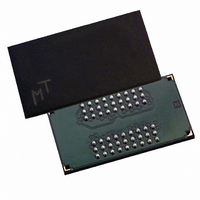
MT48H32M16LFCJ-75 L IT:A TR Micron Technology Inc, MT48H32M16LFCJ-75 L IT:A TR Datasheet - Page 45

MT48H32M16LFCJ-75 L IT:A TR
Manufacturer Part Number
MT48H32M16LFCJ-75 L IT:A TR
Description
IC SDRAM 512MBIT 133MHZ 54VBGA
Manufacturer
Micron Technology Inc
Datasheet
1.MT48H16M32LFCM-75_ITA_TR.pdf
(73 pages)
Specifications of MT48H32M16LFCJ-75 L IT:A TR
Format - Memory
RAM
Memory Type
Mobile SDRAM
Memory Size
512M (32Mx16)
Speed
133MHz
Interface
Parallel
Voltage - Supply
1.7 V ~ 1.95 V
Operating Temperature
-40°C ~ 85°C
Package / Case
54-VFBGA
Lead Free Status / RoHS Status
Lead free / RoHS Compliant
Other names
557-1331-2
PDF: 09005aef81ca5de4/Source: 09005aef81ca5e03
MT48H32M16LF_1.fm - Rev. J 2/08 EN
10. Burst in bank n continues as initiated.
11. For a WRITE without auto precharge interrupted by a READ (with or without auto pre-
12. For a WRITE without auto precharge interrupted by a WRITE (with or without auto pre-
13. Concurrent auto precharge: Bank n will initiate the auto precharge command when its
14. For a READ with auto precharge interrupted by a READ (with or without auto precharge),
15. For a READ with auto precharge interrupted by a WRITE (with or without auto precharge),
16. For a WRITE with auto precharge interrupted by a READ (with or without auto precharge),
17. For a WRITE with auto precharge interrupted by a WRITE (with or without auto precharge),
5. A BURST TERMINATE command cannot be issued to another bank; it applies to the bank
6. All states and sequences not shown are illegal or reserved.
7. READs or WRITEs to bank m listed in the Command (Action) column include READs or
8. For a READ without auto precharge interrupted by a READ (with or without auto pre-
9. For a READ without auto precharge interrupted by a WRITE (with or without auto pre-
represented by the current state only.
WRITEs with auto precharge enabled and READs or WRITEs with auto precharge disabled.
charge), the READ to bank m will interrupt the READ on bank n, CL later (Figure 11 on
page 24).
charge), the WRITE to bank m will interrupt the READ on bank n when registered. DQM
should be used one clock prior to the WRITE command to prevent bus contention.
charge), the READ to bank m will interrupt the WRITE on bank n when registered, with the
data-out appearing CL later. The last valid WRITE to bank n will be data-in registered one
clock prior to the READ to bank m.
charge), the WRITE to bank will interrupt the WRITE on bank n when registered. The last
valid WRITE to bank n will be data-in registered one clock prior to the READ to bank m.
burst has been interrupted by bank m burst.
the READ to bank m will interrupt the READ on bank n, CL later. The PRECHARGE to bank n
will begin when the READ to bank m is registered.
the WRITE to bank m will interrupt the READ on bank n when registered. DQM should be
used two clocks prior to the WRITE command to prevent bus contention. The PRECHARGE
to bank n will begin when the WRITE to bank m is registered.
the READ to bank m will interrupt the WRITE on bank n when registered, with the data-out
appearing CL later. The PRECHARGE to bank n will begin after
begins when the READ to bank m is registered. The last valid WRITE bank n will be data-in
registered one clock prior to the READ to bank m.
the WRITE to bank m interrupt the WRITE on bank n when registered. The PRECHARGE to
bank n will begin after
tered. The last valid WRITE to bank n will be data registered one clock to the WRITE to
bank m.
512Mb: 32 Meg x 16, 16 Meg x 32 Mobile SDRAM
t
WR is met, where
45
Micron Technology, Inc., reserves the right to change products or specifications without notice.
t
WR begins when the WRITE to bank m is regis-
t
WR is met, where
©2005 Micron Technology, Inc. All rights reserved.
Truth Tables
t
WR


