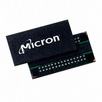
MT41J128M8HX-187E:D TR Micron Technology Inc, MT41J128M8HX-187E:D TR Datasheet - Page 131

MT41J128M8HX-187E:D TR
Manufacturer Part Number
MT41J128M8HX-187E:D TR
Description
IC DDR3 SDRAM 1GBIT 78FBGA
Manufacturer
Micron Technology Inc
Datasheet
1.MT41J64M16LA-187EB_TR.pdf
(181 pages)
Specifications of MT41J128M8HX-187E:D TR
Format - Memory
RAM
Memory Type
DDR3 SDRAM
Memory Size
1G (128M x 8)
Speed
533MHz
Interface
Parallel
Voltage - Supply
1.425 V ~ 1.575 V
Operating Temperature
0°C ~ 95°C
Package / Case
78-FBGA
Lead Free Status / RoHS Status
Lead free / RoHS Compliant
Other names
557-1377-1
- Current page: 131 of 181
- Download datasheet (9Mb)
Figure 70: Consecutive READ Bursts (BL8)
Figure 71: Consecutive READ Bursts (BC4)
Command 1
DQS, DQS#
Command 1
DQS, DQS#
Address 2
Address 2
DQ 3
DQ 3
CK#
CK#
CK
CK
READ
Bank,
READ
Col n
Bank,
Col n
T0
T0
Notes:
Notes:
NOP
NOP
T1
T1
1. NOP commands are shown for ease of illustration; other commands may be valid at these times.
2. The BL8 setting is activated by either MR0[1:0] = 00 or MR0[1:0] = 01 and A12 = 1 during READ command at T0 and T4.
3. DO n (or b) = data-out from column n (or column b).
4. BL8, RL = 5 (CL = 5, AL = 0).
1. NOP commands are shown for ease of illustration; other commands may be valid at these times.
2. The BC4 setting is activated by either MR0[1:0] = 10 or MR0[1:0] = 01 and A12 = 0 during READ command at T0 and T4.
3. DO n (or b) = data-out from column n (or column b).
4. BC4, RL = 5 (CL = 5, AL = 0).
t CCD
t CCD
NOP
NOP
T2
T2
RL = 5
RL = 5
NOP
NOP
T3
T3
READ
READ
Bank,
Col b
Bank,
Col b
T4
T4
t RPRE
t RPRE
NOP
NOP
T5
T5
DO
DO
n
n
n + 1
n + 1
DO
DO
NOP
NOP
T6
T6
n + 2
n + 2
DO
DO
RL = 5
RL = 5
t RPST
n + 3
n + 3
DO
DO
NOP
NOP
T7
T7
n + 4
DO
n + 5
DO
NOP
NOP
T8
T8
n + 6
DO
t RPRE
n + 7
DO
NOP
NOP
T9
T9
DO
DO
b
b
b + 1
b + 1
DO
DO
NOP
T10
T10
NOP
b + 2
b + 2
DO
DO
t RPST
b + 3
b + 3
DO
DO
NOP
NOP
T11
T11
b + 4
DO
b + 5
DO
NOP
T12
NOP
T12
Transitioning Data
Transitioning Data
b + 6
DO
t RPST
b + 7
DO
NOP
T13
T13
NOP
Don’t Care
Don’t Care
NOP
NOP
T14
T14
Related parts for MT41J128M8HX-187E:D TR
Image
Part Number
Description
Manufacturer
Datasheet
Request
R

Part Number:
Description:
IC DDR3 SDRAM 1GBIT 78FBGA
Manufacturer:
Micron Technology Inc
Datasheet:

Part Number:
Description:
Manufacturer:
Micron Technology Inc
Datasheet:

Part Number:
Description:
1Gb: x4, x8, x16 DDR3 SDRAM
Manufacturer:
MDTIC [Micon Design Technology Corporation]
Datasheet:

Part Number:
Description:
IC SDRAM 64MBIT 133MHZ 54TSOP
Manufacturer:
Micron Technology Inc
Datasheet:

Part Number:
Description:
IC SDRAM 64MBIT 5.5NS 86TSOP
Manufacturer:
Micron Technology Inc
Datasheet:

Part Number:
Description:
IC SDRAM 64MBIT 200MHZ 86TSOP
Manufacturer:
Micron Technology Inc
Datasheet:

Part Number:
Description:
IC SDRAM 64MBIT 133MHZ 54TSOP
Manufacturer:
Micron Technology Inc
Datasheet:

Part Number:
Description:
IC SDRAM 128MBIT 133MHZ 54TSOP
Manufacturer:
Micron Technology Inc
Datasheet:

Part Number:
Description:
IC SDRAM 256MBIT 133MHZ 90VFBGA
Manufacturer:
Micron Technology Inc
Datasheet:

Part Number:
Description:
IC SDRAM 128MBIT 133MHZ 54TSOP
Manufacturer:
Micron Technology Inc
Datasheet:

Part Number:
Description:
IC SDRAM 256MBIT 133MHZ 54TSOP
Manufacturer:
Micron Technology Inc
Datasheet:

Part Number:
Description:
IC DDR SDRAM 512MBIT 6NS 66TSOP
Manufacturer:
Micron Technology Inc
Datasheet:

Part Number:
Description:
IC SDRAM 128MBIT 167MHZ 86TSOP
Manufacturer:
Micron Technology Inc
Datasheet:

Part Number:
Description:
IC SDRAM 128MBIT 143MHZ 86TSOP
Manufacturer:
Micron Technology Inc
Datasheet:

Part Number:
Description:
SDRAM 256M-BIT 1.8V 54-PIN VFBGA
Manufacturer:
Micron Technology Inc
Datasheet:


