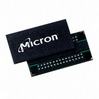
MT41J128M8HX-187E:D TR Micron Technology Inc, MT41J128M8HX-187E:D TR Datasheet - Page 40

MT41J128M8HX-187E:D TR
Manufacturer Part Number
MT41J128M8HX-187E:D TR
Description
IC DDR3 SDRAM 1GBIT 78FBGA
Manufacturer
Micron Technology Inc
Datasheet
1.MT41J64M16LA-187EB_TR.pdf
(181 pages)
Specifications of MT41J128M8HX-187E:D TR
Format - Memory
RAM
Memory Type
DDR3 SDRAM
Memory Size
1G (128M x 8)
Speed
533MHz
Interface
Parallel
Voltage - Supply
1.425 V ~ 1.575 V
Operating Temperature
0°C ~ 95°C
Package / Case
78-FBGA
Lead Free Status / RoHS Status
Lead free / RoHS Compliant
Other names
557-1377-1
- Current page: 40 of 181
- Download datasheet (9Mb)
Electrical Specifications – DC and AC
DC Operating Conditions
Table 20:
Input Operating Conditions
Table 21:
PDF: 09005aef826aa906/Source: 09005aef82a357c3
1Gb_DDR3_3.fm - Rev. F 11/08 EN
Parameter/Condition
Parameter/Condition
Supply voltage
I/O supply voltage
Input leakage current
Any input 0V ≤ V
(All other pins not under test = 0V)
V
V
(All other pins not under test = 0V)
Input reference voltage command/address bus
I/O reference voltage DQ bus
Command/address termination voltage
(system level, not direct DRAM input)
REF
REF
DQ = V
supply leakage current
DD
DC Electrical Characteristics and Operating Conditions
All voltages are referenced to V
DC Electrical Characteristics and Input Conditions
All voltages are referenced to V
/2 or V
IN
Notes:
Notes:
≤ V
REF
DD
CA = V
, V
REF
1. V
2. V
3. V
4. The minimum limit requirement is for testing purposes. The leakage current on the V
1. V
2. DC values are determined to be less than 20 MHz in frequency. DRAM must meet specifica-
3. V
4. V
DD
pin 0V ≤ V
(0Hz to 250 kHz) specifications. V
parameters.
should be minimal.
Externally generated peak noise (noncommon mode) on V
× V
percent of V
tions if the DRAM induces additional AC noise greater than 20 MHz in frequency.
level. Externally generated peak noise (noncommon mode) on V
percent × V
exceed ±2 percent of V
tors. MIN and MAX values are system-dependent.
/2
DD
DD
REF
REF
REF
TT
DD
is not applied directly to the device. V
CA(
DQ(
and V
and V
(see Table 21).
around the V
DC
DC
IN
) is expected to be approximately 0.5 × V
DD
DD
) is expected to be approximately 0.5 × V
DD
≤ 1.1V
REF
Q must track one another. V
Q may include AC noise of ±50mV (250 kHz to 20 MHz) in addition to the DC
SS
SS
around the V
CA(
DC
V
V
REF
Symbol
REF
REF
).
Symbol
CA(
REF
V
DQ(
V
CA(
I
V
TT
VREF
DD
DQ(
DD
I
DC
I
DC
DC
Q
REF
) value. Peak-to-peak AC noise on V
40
)
)
DC
DQ(
).
DD
0.49 × V
0.49 × V
DC
and V
1.425
1.425
) value. Peak-to-peak AC noise on V
Min
Min
–2
–1
Micron Technology, Inc., reserves the right to change products or specifications without notice.
–
Electrical Specifications – DC and AC
DD
TT
DD
DD
DD
Q must be less than or equal to V
is a system supply for signal termination resis-
Q must be at same level for valid AC timing
0.5 × V
1Gb: x4, x8, x16 DDR3 SDRAM
0.5 × V
0.5 × V
Nom
DD
Nom
1.5
1.5
DD
–
–
and to track variations in the DC level.
and to track variations in the DC
DD
DD
DD
Q
REF
CA may not exceed ±1 percent
0.51 × V
0.51 × V
REF
©2006 Micron Technology, Inc. All rights reserved.
1.575
1.575
Max
REF
Max
2
1
CA should not exceed ±2
–
DQ may not exceed ±1
DD
DD
REF
Units
DQ should not
Units
DD
µA
µA
V
V
V
V
V
. V
SS
Notes
Notes
= V
REF
1, 2
1, 2
3, 4
1, 2
2, 3
4
SS
pin
Q.
Related parts for MT41J128M8HX-187E:D TR
Image
Part Number
Description
Manufacturer
Datasheet
Request
R

Part Number:
Description:
IC DDR3 SDRAM 1GBIT 78FBGA
Manufacturer:
Micron Technology Inc
Datasheet:

Part Number:
Description:
Manufacturer:
Micron Technology Inc
Datasheet:

Part Number:
Description:
1Gb: x4, x8, x16 DDR3 SDRAM
Manufacturer:
MDTIC [Micon Design Technology Corporation]
Datasheet:

Part Number:
Description:
IC SDRAM 64MBIT 133MHZ 54TSOP
Manufacturer:
Micron Technology Inc
Datasheet:

Part Number:
Description:
IC SDRAM 64MBIT 5.5NS 86TSOP
Manufacturer:
Micron Technology Inc
Datasheet:

Part Number:
Description:
IC SDRAM 64MBIT 200MHZ 86TSOP
Manufacturer:
Micron Technology Inc
Datasheet:

Part Number:
Description:
IC SDRAM 64MBIT 133MHZ 54TSOP
Manufacturer:
Micron Technology Inc
Datasheet:

Part Number:
Description:
IC SDRAM 128MBIT 133MHZ 54TSOP
Manufacturer:
Micron Technology Inc
Datasheet:

Part Number:
Description:
IC SDRAM 256MBIT 133MHZ 90VFBGA
Manufacturer:
Micron Technology Inc
Datasheet:

Part Number:
Description:
IC SDRAM 128MBIT 133MHZ 54TSOP
Manufacturer:
Micron Technology Inc
Datasheet:

Part Number:
Description:
IC SDRAM 256MBIT 133MHZ 54TSOP
Manufacturer:
Micron Technology Inc
Datasheet:

Part Number:
Description:
IC DDR SDRAM 512MBIT 6NS 66TSOP
Manufacturer:
Micron Technology Inc
Datasheet:

Part Number:
Description:
IC SDRAM 128MBIT 167MHZ 86TSOP
Manufacturer:
Micron Technology Inc
Datasheet:

Part Number:
Description:
IC SDRAM 128MBIT 143MHZ 86TSOP
Manufacturer:
Micron Technology Inc
Datasheet:

Part Number:
Description:
SDRAM 256M-BIT 1.8V 54-PIN VFBGA
Manufacturer:
Micron Technology Inc
Datasheet:


