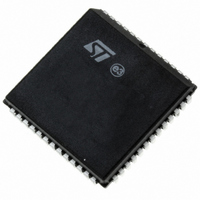
DSM2180F3V-15K6 STMicroelectronics, DSM2180F3V-15K6 Datasheet - Page 24

DSM2180F3V-15K6
Manufacturer Part Number
DSM2180F3V-15K6
Description
IC FLASH 1MBIT 150NS 52PLCC
Manufacturer
STMicroelectronics
Specifications of DSM2180F3V-15K6
Format - Memory
FLASH
Memory Type
FLASH
Memory Size
1M (128K x 8)
Speed
150ns
Interface
Parallel
Voltage - Supply
3 V ~ 3.6 V
Operating Temperature
-40°C ~ 85°C
Package / Case
52-PLCC
Operating Supply Voltage (typ)
3.3V
Operating Supply Voltage (min)
2.97V
Operating Supply Voltage (max)
3.63V
Mounting
Surface Mount
Pin Count
52
Lead Free Status / RoHS Status
Lead free / RoHS Compliant
Other names
497-1336-5
Available stocks
Company
Part Number
Manufacturer
Quantity
Price
Company:
Part Number:
DSM2180F3V-15K6
Manufacturer:
FREESCALE
Quantity:
101
Company:
Part Number:
DSM2180F3V-15K6
Manufacturer:
STMicroelectronics
Quantity:
10 000
DSM2180F3V
Flash memory sector may be suspended, in order
to read data from another Flash memory sector,
and then resumed.
The address provided with the initial Flash Sector
Erase command sequence (Table 5) must select
the first desired sector (FS0 - FS7) to erase. Sub-
sequent sector erase commands that are append-
ed on within the time-out period must be
addressed to other desired segments (FS0 - FS7).
Suspend Sector Erase. When a Sector Erase
cycle is in progress, the Suspend Sector Erase in-
struction sequence can be used to suspend the
cycle by writing 0B0h to any address when an ap-
propriate Sector Select (FS0-FS7) is selected
(See Table 5). This allows reading of data from an-
other Flash memory sector after the Erase cycle
has been suspended. Suspend Sector Erase is
accepted only during an Erase cycle and defaults
to Read mode. A Suspend Sector Erase instruc-
tion sequence executed during an Erase time-out
period, in addition to suspending the Erase cycle,
terminates the time out period.
The Toggle Flag (DQ6) bit stops toggling when the
device internal logic is suspended. The status of
this bit must be monitored at an address within the
Flash memory sector being erased. The Toggle
Flag (DQ6) bit stops toggling between 0.1 µs and
15 µs after the Suspend Sector Erase instruction
sequence has been executed. The device is then
automatically set to Read mode.
If an Suspend Sector Erase instruction sequence
was executed, the following rules apply:
– Attempting to read from a Flash memory sector
– Reading from a Flash memory sector that was
Table 7. Sector Protection/Security Bit Definition – Flash Protection Register
Note: 1. Bit Definitions:
Table 8. Security Bit Definition
Note: 1. Bit Definitions:
24/63
Bit 7
Sec7_Prot
Bit 7
Security_Bit
that was being erased outputs invalid data.
not being erased is valid.
Sec<i>_Prot 1 = Flash memory sector <i> is write protected.
Sec<i>_Prot 0 = Flash memory sector <i> is not write protected.
1 = Security Bit in device has been set.
Bit 6
Sec6_Prot
Bit 6
not used
Bit 5
Bit 5
Sec5_Prot
not used
Bit 4
Sec4_Prot
Bit 4
not used
Bit 3
Bit 3
Sec3_Prot
not used
– The Flash memory cannot be programmed, and
– If a Reset Flash instruction sequence is re-
Resume Sector Erase. If a Suspend Sector
Erase instruction sequence was previously exe-
cuted, the erase cycle may be resumed with this
instruction sequence. The Resume Sector Erase
instruction sequence consists of writing 030h to
any address while an appropriate Sector Select
(FS0-FS7) is active. (See Table 5.)
Flash Memory Sector Protect.
Each Flash memory sector can be separately pro-
tected against Program and Erase cycles. Sector
Protection provides additional data security be-
cause it disables all Program or Erase cycles. This
mode can be activated through the JTAG Port or a
Device Programmer. Sector protection can be se-
lected for each sector using PSDsoft Express.
This automatically protects selected sectors when
the device is programmed through the JTAG Port
or a Device Programmer. Flash memory sectors
can be unprotected to allow updating of their con-
tents using the JTAG Port or a Device Program-
mer. The DSP can read (but cannot change) the
sector protection bits.
Any attempt to program or erase a protected Flash
memory sector is ignored by the device. The Verify
operation results in a read of the protected data.
This allows a guarantee of the retention of the Pro-
tection status.
The sector protection status can be read by the
DSP through the Flash memory protection regis-
ters (in the csiop block) as defined in Table 7.
only responds to Resume Sector Erase and Re-
set Flash instruction sequences (Read is an op-
eration and is allowed).
ceived, data in the Flash memory sector that
was being erased is invalid.
Bit 2
Sec2_Prot
Bit 2
not used
Bit 1
Sec1_Prot
Bit 1
not used
Bit 0
Sec0_Prot
Bit 0
not used


