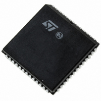
DSM2180F3V-15K6 STMicroelectronics, DSM2180F3V-15K6 Datasheet - Page 40

DSM2180F3V-15K6
Manufacturer Part Number
DSM2180F3V-15K6
Description
IC FLASH 1MBIT 150NS 52PLCC
Manufacturer
STMicroelectronics
Specifications of DSM2180F3V-15K6
Format - Memory
FLASH
Memory Type
FLASH
Memory Size
1M (128K x 8)
Speed
150ns
Interface
Parallel
Voltage - Supply
3 V ~ 3.6 V
Operating Temperature
-40°C ~ 85°C
Package / Case
52-PLCC
Operating Supply Voltage (typ)
3.3V
Operating Supply Voltage (min)
2.97V
Operating Supply Voltage (max)
3.63V
Mounting
Surface Mount
Pin Count
52
Lead Free Status / RoHS Status
Lead free / RoHS Compliant
Other names
497-1336-5
Available stocks
Company
Part Number
Manufacturer
Quantity
Price
Company:
Part Number:
DSM2180F3V-15K6
Manufacturer:
FREESCALE
Quantity:
101
Company:
Part Number:
DSM2180F3V-15K6
Manufacturer:
STMicroelectronics
Quantity:
10 000
DSM2180F3V
PLD Power Management
The power and speed of the PLDs are controlled
by the Turbo bit (bit 3) in the PMMR0. By setting
the bit to 1, the Turbo mode is off and the PLDs
consume the specified stand-by current when the
inputs are not switching for an extended time of
100 ns. The propagation delay time is increased
by 10 ns after the Turbo bit is set to 1 (turned off)
when the inputs change at a composite frequency
Table 18. Power Management Mode Registers PMMR2
Note: 1. The bits of this register are cleared to zero following Power-up. Subsequent Reset (Reset) pulses do not clear the registers.
PSD Chip Select Input (CSI, PD2)
PD2 of Port D can be configured in PSDsoft Ex-
press as PSD Chip Select Input (
the signal selects and enables the internal Flash
memory and I/O blocks for Read or Write opera-
tions involving the device. A High on PSD Chip Se-
lect Input (
and reduces the device power consumption. How-
ever, the PLD and I/O signals remain operational
when PSD Chip Select Input (
There may be a timing penalty when using PSD
Chip Select Input (
speed grade of the device that you are using. See
the timing parameter t
Input Clock. The device provides the option to
block CLKIN (PD1) from reaching the PLDs to
save AC power consumption. CLKIN (PD1) is an
input to the PLD AND Array and the OMCs.
If CLKIN (PD1) is not being used as part of the
PLD logic equation, the clock should be blocked to
save AC power. CLKIN (PD1) is disconnected
40/63
Bit 0
Bit 1
Bit 2
Bit 3
Bit 4
Bit 5
Bit 6
Bit 7
X
X
PLD Array
CNTL0
PLD Array
CNTL1
PLD Array
CNTL2
PLD Array
PD0
PLD Array
PC7
X
CSI
, PD2) disables the Flash memory
CSI
SLQV
0
0
0 = on Cntl0 input to the PLD AND Array is passed onto PLDs.
1 = off Cntl0 input to PLD AND Array is blocked, saving power.
0 = on Cntl1 input to the PLD AND Array is passed onto PLDs.
1 = off Cntl1 input to PLD AND Array is blocked, saving power.
0 = on Cntl2 input to the PLD AND Array is passed onto PLDs.
1 = off Cntl2 input to PLD AND Array is blocked, saving power.
0 = on PD0 input to the PLD AND Array is passed onto PLDs.
1 = off PD0 input to PLD AND Array is blocked, saving power.
0 = on PC7 input to the PLD AND Array is passed onto PLDs.
1 = off PC7 input to PLD AND Array is blocked, saving power.
0
, PD2) depending on the
in Table 31.
CSI
Not used, and should be set to zero.
Not used, and should be set to zero.
Not used, and should be set to zero.
CSI
, PD2) is High.
). When Low,
of less than 10 MHz. When the Turbo bit is reset to
0 (turned on), the PLDs run at full power and
speed. The Turbo bit affects the PLD’s DC power,
AC power, and propagation delay.
Blocking MCU control signals with the bits of the
PMMR registers can further reduce PLD AC power
consumption by lowering the effective composite
frequency of inputs to the PLDs.
from the PLD AND Array or the Macrocells block
by setting bits 4 or 5 to a 1 in PMMR0.
Input Control Signals. The device provides the
option to block the input control signals (CNTL0,
CNTL1, CNTL2, PD0, and PC7) from reaching the
PLDs to save AC power consumption. These con-
trol signals are inputs to the PLD AND Array. If any
of these are not being used as part of the PLD log-
ic equation, these control signals should be dis-
abled to save AC power. They are disconnected
from the PLD AND Array by setting bits 2, 3, 4, 5,
and 6 to a 1 in the PMMR2 register. Note: CNTL0
and CNTL1 (DSP
nently routed to the Flash memory array and can-
not be blocked from the array by the PMMR
registers (that’s why WR and RD signals do not
have to be specified in PSDsoft Express for Flash
memory segment chip-select equations for FS0 -
FS7). CNTL0 and CNTL1 are blocked from the
PLDs with PMMR registers bits when these sig-
nals are specifically used in logic equations speci-
fied in PSDsoft Express.
1
WR
and DSP
RD
) are perma-


