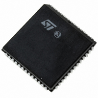
DSM2180F3V-15K6 STMicroelectronics, DSM2180F3V-15K6 Datasheet - Page 42

DSM2180F3V-15K6
Manufacturer Part Number
DSM2180F3V-15K6
Description
IC FLASH 1MBIT 150NS 52PLCC
Manufacturer
STMicroelectronics
Specifications of DSM2180F3V-15K6
Format - Memory
FLASH
Memory Type
FLASH
Memory Size
1M (128K x 8)
Speed
150ns
Interface
Parallel
Voltage - Supply
3 V ~ 3.6 V
Operating Temperature
-40°C ~ 85°C
Package / Case
52-PLCC
Operating Supply Voltage (typ)
3.3V
Operating Supply Voltage (min)
2.97V
Operating Supply Voltage (max)
3.63V
Mounting
Surface Mount
Pin Count
52
Lead Free Status / RoHS Status
Lead free / RoHS Compliant
Other names
497-1336-5
Available stocks
Company
Part Number
Manufacturer
Quantity
Price
Company:
Part Number:
DSM2180F3V-15K6
Manufacturer:
FREESCALE
Quantity:
101
Company:
Part Number:
DSM2180F3V-15K6
Manufacturer:
STMicroelectronics
Quantity:
10 000
DSM2180F3V
ISP programming time can be reduced as much as
30% by using two more signals on Port C, TSTAT
and TERR in addition to TMS, TCK, TDI and TDO.
See Table 20. The FlashLINK
ming cable available from STMicroelectronics for
$59USD and PSDsoft Express software that is
available at no charge from www.psdst.com is all
that is needed to program a DSM device using the
parallel port on any PC or laptop.
By default, the four pins on Port C are enabled for
the basic JTAG signals TMS, TCK, TDI, and TDO
on a blank device (and as shipped from factory)
See Application Note AN1153 for more details on
JTAG In-System Programming (ISP).
Standard JTAG Signals. The standard JTAG
signals (TMS, TCK, TDI, and TDO) can be en-
abled by any of three different conditions that are
logically ORed. When enabled, TDI, TDO, TCK,
and TMS are inputs, waiting for a JTAG serial
command from an external JTAG controller device
(such as FlashLINK or Automated Test Equip-
ment). When the enabling command is received,
TDO becomes an output and the JTAG channel is
fully functional inside the device. The same com-
mand that enables the JTAG channel may option-
ally enable the two additional JTAG signals,
TSTAT and TERR.
The following symbolic logic equation specifies the
conditions enabling the four basic JTAG signals
(TMS, TCK, TDI, and TDO) on their respective
Port C pins. For purposes of discussion, the logic
label JTAG_ON is used. When JTAG_ON is true,
the four pins are enabled for JTAG operation.
When JTAG_ON is false, the four pins can be
used for general device I/O as specified in PSD-
soft Express. JTAG_ON can become true by any
of three different ways as shown:
JTAG_ON =
1. PSDsoft Express Pin Configuration -OR-
2. PSDsoft Express PLD equation -OR-
3. DSP writes to register in csiop block
Method 1 is most common. This is when the JTAG
pins are selected in PSDsoft Express to be “dedi-
cated” JTAG pins. They can always transmit and
receive JTAG information because they are “full-
time” JTAG pins.
Method 2 is used only when the JTAG pins are
multiplexed with general I/O functions. For de-
signs that need every I/O pin, the JTAG pins may
be used for general I/O when they are not used for
ISP. However, when JTAG pins are multiplexed
with general I/O functions, the designer must in-
clude a way to get the pins back into JTAG mode
when it is time for JTAG operations again. In this
42/63
TM
JTAG
program-
case, a single PLD input from Ports B, C, or D
must be dedicated to switch the Port C pins from I/
O mode back to ISP mode at any time. It is recom-
mended to physically connect this dedicated PLD
input pin to the JEN\ output signal from the Flash-
link cable when multiplexing JTAG signals. See
Application Note AN1153 for details.
Method 3 is rarely used to control JTAG pin oper-
ation. The DSP can set the port C pins to function
as JTAG ISP by setting the JTAG Enable bit in a
register of the csiop block, but as soon as the DSM
chip is reset, the csiop block registers are cleared,
which turns off the JTAG-ISP function. Controlling
JTAG pins using this method is not recommended.
Table 20. JTAG Port Signals
JTAG Extensions. TSTAT and TERR are two
JTAG extension signals (must be used as a pair)
enabled by a command received over the four
standard JTAG signals (TMS, TCK, TDI, and
TDO) by PSDsoft Express. They are used to
speed Program and Erase cycles by indicating
status on device pins instead of having to scan the
status out serially using the standard JTAG chan-
nel. See Application Note AN1153.
TERR indicates if an error has occurred when
erasing a sector or programming a byte in Flash
memory. This signal goes Low (active) when an
Error condition occurs.
TSTAT behaves the same as Ready/Busy de-
scribed previously.
the device is in Read mode (Flash memory con-
tents can be read).
memory Program or Erase cycles are in progress.
TSTAT and TERR can be configured as open-
drain type signals with PSDsoft Express. This fa-
cilitates a wired-OR connection of TSTAT signals
from multiple DSM2180F3V devices and a wired-
OR connection of TERR signals from those same
devices. This is useful when several devices are
“chained” together in a JTAG environment. PSD-
soft Express puts TSTAT and TERR signals to
open-drain by default. Click on 'Properties' in the
JTAG-ISP window of PSDsoft Express to change
to standard CMOS push-pull. It is recommended
PC0
PC1
PC3
PC4
PC5
PC6
Port C Pin
TMS
TCK
TSTAT
TERR
TDI
TDO
JTAG Signals
TSTAT
TSTAT
is inactive logic 1 when
is logic 0 when Flash
Mode Select
Clock
Status
Error Flag
Serial Data In
Serial Data Out
Description


