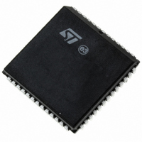
DSM2180F3V-15K6 STMicroelectronics, DSM2180F3V-15K6 Datasheet - Page 25

DSM2180F3V-15K6
Manufacturer Part Number
DSM2180F3V-15K6
Description
IC FLASH 1MBIT 150NS 52PLCC
Manufacturer
STMicroelectronics
Specifications of DSM2180F3V-15K6
Format - Memory
FLASH
Memory Type
FLASH
Memory Size
1M (128K x 8)
Speed
150ns
Interface
Parallel
Voltage - Supply
3 V ~ 3.6 V
Operating Temperature
-40°C ~ 85°C
Package / Case
52-PLCC
Operating Supply Voltage (typ)
3.3V
Operating Supply Voltage (min)
2.97V
Operating Supply Voltage (max)
3.63V
Mounting
Surface Mount
Pin Count
52
Lead Free Status / RoHS Status
Lead free / RoHS Compliant
Other names
497-1336-5
Available stocks
Company
Part Number
Manufacturer
Quantity
Price
Company:
Part Number:
DSM2180F3V-15K6
Manufacturer:
FREESCALE
Quantity:
101
Company:
Part Number:
DSM2180F3V-15K6
Manufacturer:
STMicroelectronics
Quantity:
10 000
DSM Security Bit
A programmable security bit in the DSM protects
its contents from unauthorized viewing and copy-
ing. When set, the security bit will block access of
programming devices (JTAG or others) to the
DSM Flash memory and PLD configuration. The
only way to defeat the security bit is to erase the
entire DSM device, after which the device is blank
and may be used again. The DSP will always have
access to Flash memory contents through the 8-bit
data port even while the security bit is set. The
DSP can read the status of the security bit (but it
cannot change it) by reading the Device Security
register in the csiop block as defined in Table 8.
Reset Flash
The Reset Flash instruction sequence resets the
internal memory logic state machine and puts
Flash memory into Read Array mode. It consists of
one write cycle (see Table 5). It must be executed
after:
– Reading the Flash Protection Status or Flash ID
– An Error condition has occurred (and the device
The Reset Flash instruction sequence puts the
Flash memory back into normal Read Array mode.
It may take the Flash memory up to a few millisec-
onds to complete the Reset cycle. The Reset
Flash instruction sequence is ignored when it is is-
sued during a Program or Bulk Erase cycle of the
Flash memory. The Reset Flash instruction se-
quence aborts any on-going Sector Erase cycle,
and returns the Flash memory to the normal Read
Array mode within a few milliseconds.
Page Register
The 8-bit Page Register increases the addressing
capability of the DSP by a factor of up to 256. The
contents of the register can also be read by the
DSP. The outputs of the Page Register (PG0-
PG7) are inputs to the DPLD decoder and can be
included in the Sector Select (FS0-FS7) equa-
tions. See Figure 12.
If memory paging is not needed, or if not all 8 page
register bits are needed for memory paging, then
these bits may be used in the CPLD for general
logic. The eight flip-flops in the register are con-
nected to the internal data bus D0-D7. The DSP
can write to or read from the Page Register. The
Page Register can be accessed at address loca-
tion csiop + E0h. Page Register outputs are
cleared to logic 0 at reset.
has set the Error Flag (DQ5) bit to 1) during a
Flash memory Program or Erase cycle.
Figure 12. Page Register
PLDs
The PLDs bring programmable logic to the device.
After specifying the logic for the PLDs using PSD-
soft Express, the logic is programmed into the de-
vice and available upon Power-up.
The PLDs have selectable levels of performance
and power consumption.
The device contains two PLDs: the Decode PLD
(DPLD), and the Complex PLD (CPLD), as shown
in Figure 13.
Table 9. DPLD and CPLD Inputs
Note: 1. DSP address lines A16, A17, and others may enter the
DSP Address Bus
DSP Control Signals
Reset
PortB Input Macrocells
PortC Input Macrocells PC7-PC0
Port D Inputs
Page Register
Macrocell AB
Feedback
Macrocell BC
Feedback
Flash memory
Program Status Bit
Input Source
2. Additional DSP control signals may enter the DMS device
DSM device on any pin on ports B, C, or D. See Figure 6
for recommended connections.
on any pin on Ports B, C, or D. See Figure 6 for recom-
mended connections.
RESET
D0 - D7
R/W
D0
D1
D2
D3
D4
D5
D6
D7
REGISTER
PAGE
1
2
Q0
Q1
Q2
Q3
Q4
Q5
Q6
Q7
A15-A0
CNTL2-CNTL0
RST
PB7-PB0
PD2-PD0
PG7-PG0
MCELLAB FB7-0
MCELLBC FB7-0
Ready/Busy
PGR0
PGR1
PGR2
PGR3
PGR4
PGR5
PGR6
PGR7
Input Name
DPLD
CPLD
AND
PLD
DSM2180F3V
16
3
1
8
8
3
8
8
8
1
INTERNAL
SELECTS
AND LOGIC
Number
Signals
of
25/63


