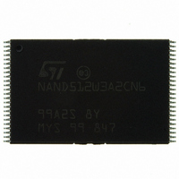
NAND512W3A2CN6E NUMONYX, NAND512W3A2CN6E Datasheet - Page 32

NAND512W3A2CN6E
Manufacturer Part Number
NAND512W3A2CN6E
Description
IC FLASH 512MBIT 48TSOP
Manufacturer
NUMONYX
Datasheet
1.NAND512R3A2CZA6E.pdf
(55 pages)
Specifications of NAND512W3A2CN6E
Format - Memory
FLASH
Memory Type
FLASH - Nand
Memory Size
512M (64M x 8)
Interface
Parallel
Voltage - Supply
2.7 V ~ 3.6 V
Operating Temperature
-40°C ~ 85°C
Package / Case
48-TSOP
Cell Type
NAND
Density
512Mb
Access Time (max)
12us
Interface Type
Parallel
Boot Type
Not Required
Address Bus
26b
Operating Supply Voltage (typ)
3/3.3V
Operating Temp Range
-40C to 85C
Package Type
TSOP
Program/erase Volt (typ)
2.7 to 3.6V
Sync/async
Asynchronous
Operating Temperature Classification
Industrial
Operating Supply Voltage (min)
2.7V
Operating Supply Voltage (max)
3.6V
Word Size
8b
Number Of Words
64M
Supply Current
20mA
Mounting
Surface Mount
Pin Count
48
Lead Free Status / RoHS Status
Lead free / RoHS Compliant
Speed
-
Lead Free Status / RoHS Status
Lead free / RoHS Compliant, Compliant
Available stocks
Company
Part Number
Manufacturer
Quantity
Price
Company:
Part Number:
NAND512W3A2CN6E
Manufacturer:
MICRON
Quantity:
1 500
Part Number:
NAND512W3A2CN6E
Manufacturer:
ST
Quantity:
20 000
Software algorithms
7.3
7.4
7.5
32/55
Garbage collection
When a data page needs to be modified, it is faster to write to the first available page, and
the previous page is marked as invalid. After several updates it is necessary to remove
invalid pages to free some memory space.
To free this memory space and allow further program operations it is recommended to
implement a garbage collection algorithm. In a garbage collection software the valid pages
are copied into a free area and the block containing the invalid pages is erased (see
Figure
Figure 17. Garbage collection
Wear-leveling algorithm
For write-intensive applications, it is recommended to implement a wear-leveling algorithm
to monitor and spread the number of write cycles per block.
In memories that do not use a wear-leveling algorithm not all blocks get used at the same
rate.
The wear-leveling algorithm ensures that equal use is made of all the available write cycles
for each block. There are two wear-leveling levels:
The second level wear-leveling is triggered when the difference between the maximum and
the minimum number of write cycles per block reaches a specific threshold.
Error correction code
An error correction code (ECC) can be implemented in the NAND flash memories to identify
and correct errors in the data.
For every 2048 bits in the device the implementation of 22 bits of ECC (16 bits for line parity
plus 6 bits for column parity) is required.
First level wear-leveling, new data is programmed to the free blocks that have had the
fewest write cycles
Second level wear-leveling, long-lived data is copied to another block so that the
original block can be used for more frequently-changed data.
17).
Invalid
Valid
page
page
Old area
(erased)
Free
page
New area (after GC)
AI07599B
NAND512-A2C


