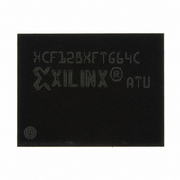
XCF128XFTG64C Xilinx Inc, XCF128XFTG64C Datasheet - Page 33

XCF128XFTG64C
Manufacturer Part Number
XCF128XFTG64C
Description
IC PROM SRL 128M GATE 64-FTBGA
Manufacturer
Xilinx Inc
Datasheet
1.XCF128XFTG64C.pdf
(88 pages)
Specifications of XCF128XFTG64C
Memory Size
128Mb
Programmable Type
In System Programmable
Voltage - Supply
1.7 V ~ 2 V
Operating Temperature
-40°C ~ 85°C
Package / Case
64-TBGA
Access Time
85ns
Supply Voltage Range
1.7V To 2V
Memory Case Style
FTBGA
No. Of Pins
64
Operating Temperature Range
-40°C To +85°C
Svhc
No SVHC (15-Dec-2010)
Package /
RoHS Compliant
Lead Free Status / RoHS Status
Lead free / RoHS Compliant
Other names
122-1578
Available stocks
Company
Part Number
Manufacturer
Quantity
Price
Company:
Part Number:
XCF128XFTG64C
Manufacturer:
XILINX
Quantity:
319
Part Number:
XCF128XFTG64C
Manufacturer:
XILINX/赛灵思
Quantity:
20 000
The Clock signal is then halted at V
Enable (G) goes High. When Output Enable goes Low
again and the Clock signal restarts, the Synchronous Burst
Read operation is resumed at its previous location.
When READY_WAIT (with CR4 = ‘0’) is gated by E, it
reverts to high impedance when G goes High.
See
Single Synchronous Read Mode
Single Synchronous Read operations are similar to
Synchronous Burst Read operations except that the
memory outputs the same data to the end of the operation.
Dual Operations and Multiple Bank Architecture
The Multiple Bank Architecture of Platform Flash XL gives
greater flexibility for software developers to split the code
and data spaces within the memory array. The Dual
Operations feature simplifies the software management of
the device by allowing code to be executed from one bank
while another bank is being programmed or erased. This
feature allows read operations with zero latency in one bank
while programming or erasing in another bank.
Note:
erase mode.
If a read operation is required in a bank which is
programming or erasing, the program or erase operation
can be suspended. Also if the suspended operation is
erase, then a program command can be issued to another
block so that the device can have one block in Erase
Table 15: Dual Operations Allowed in Another Bank
Table 16: Dual Operations Allowed in Same Bank
DS617 (v3.0.1) January 07, 2010
Product Specification
Idle
Programming
Erasing
Program Suspended
Erase Suspended
Idle
Programming
Erasing
Status of Bank
Status of Bank
Table 29, page
Only one bank at a time is allowed to be in program or
R
52, and
Array
Array
Read
Read
–
–
(1)
(1)
Figure 30, page 54
Register
Register
Status
Status
IH
Read
Read
or at V
IL
Read CFI
Read CFI
, and Output
Query
Query
for details.
Platform Flash XL High-Density Configuration and Storage Device
Commands Allowed in Another Bank
www.xilinx.com
Commands Allowed in Same Bank
Electronic
Electronic
Signature
Signature
Read
Read
Synchronous Single Reads are used to read the Electronic
Signature, Status Register, CFI, Block Protection Status,
Configuration Register Status, or Protection Register. When
the addressed bank is in Read CFI, Read Status Register,
or Read Electronic Signature mode, the READY_WAIT
signal (if configured for the Wait function with CR4 = ‘0’) is
asserted during X-latency, the WAIT state and at the end of
a 4, 8 and 16-word burst. The signal is only deasserted
when output data is valid. See
Figure 27, page
Suspend mode, one in programming mode, and other
banks in read mode.
Bus Read operations are allowed in other banks between
setup and confirm cycles of program or erase operations.
By using a combination of these features, read operations
are always possible in Platform Flash XL.
Table 15
are possible in other banks and in the same bank.
Dual operations between the Parameter Bank and either of
the CFI, OTP, or Electronic Signature memory spaces are
not allowed.
operations are allowed or not between the CFI, OTP,
Electronic Signature locations and the memory array.
Program,
Program,
Program
Program
Buffer
Buffer
and
–
–
–
–
–
Table 17, page 36
Table 16, page 35
51, for details.
Block
Erase
Block
Erase
–
–
–
–
–
–
Table 29, page 52
shows which dual
show which dual operations
Program/
Program/
Suspend
Suspend
Erase
Erase
–
–
Erase Resume
Erase Resume
Program/
Program/
and
–
–
–
–
33


