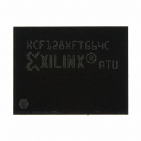
XCF128XFTG64C Xilinx Inc, XCF128XFTG64C Datasheet - Page 56

XCF128XFTG64C
Manufacturer Part Number
XCF128XFTG64C
Description
IC PROM SRL 128M GATE 64-FTBGA
Manufacturer
Xilinx Inc
Datasheet
1.XCF128XFTG64C.pdf
(88 pages)
Specifications of XCF128XFTG64C
Memory Size
128Mb
Programmable Type
In System Programmable
Voltage - Supply
1.7 V ~ 2 V
Operating Temperature
-40°C ~ 85°C
Package / Case
64-TBGA
Access Time
85ns
Supply Voltage Range
1.7V To 2V
Memory Case Style
FTBGA
No. Of Pins
64
Operating Temperature Range
-40°C To +85°C
Svhc
No SVHC (15-Dec-2010)
Package /
RoHS Compliant
Lead Free Status / RoHS Status
Lead free / RoHS Compliant
Other names
122-1578
Available stocks
Company
Part Number
Manufacturer
Quantity
Price
Company:
Part Number:
XCF128XFTG64C
Manufacturer:
XILINX
Quantity:
319
Part Number:
XCF128XFTG64C
Manufacturer:
XILINX/赛灵思
Quantity:
20 000
Table 31: Write AC Characteristics, Chip Enable Controlled
Notes:
1.
2.
X-Ref Target - Figure 33
DS617 (v3.0.1) January 07, 2010
Product Specification
Sampled only, not 100% tested.
T
should take this timing into account and can insert a software No-Op instruction to delay the first read in the same bank after issuing any
command and to delay the first read to any address after issuing a Set Configuration Register command. If the first read after the command
is a Read Array operation in a different bank and no changes to the Configuration Register are issued, T
Symbol
WHEL
T
T
T
T
T
T
T
T
T
T
T
T
T
T
T
T
T
T
T
T
T
T
T
T
AVAV
AVEH
AVLH
DVEH
EHAX
EHDX
EHEL
EHGL
EHWH
ELKV
ELEH
ELLH
ELQV
GHEL
LHAX
LLLH
WHEL
WLEL
EHVPL
EHWPL
QVVPL
QVWPL
VPHEH
WPHEH
has this value when reading in the targeted bank or when reading following a Set Configuration Register command. System designers
R
V
(2)
DD
W,E,G,L
, V
T
T
T
T
T
T
T
T
T
Alt
AH
DDQ
WC
DS
DH
CPH
CH
CP
CS
VPS
RP
Address Valid to Next Address Valid
Address Valid to Chip Enable High
Address Valid to Latch Enable High
Data Valid to Chip Enable High
Chip Enable High to Address Transition
Chip Enable High to Input Transition
Chip Enable High to Chip Enable Low
Chip Enable High to Output Enable Low
Chip Enable High to Write Enable High
Chip Enable Low to Clock Valid
Chip Enable Low to Chip Enable High
Chip Enable Low to Latch Enable High
Chip Enable Low to Output Valid
Output Enable High to Chip Enable Low
Latch Enable High to Address Transition
Latch Enable Pulse Width
Write Enable High to Chip Enable Low
Write Enable Low to Chip Enable Low
Chip Enable High to V
Chip Enable High to Write Protect Low
Output (Status Register) Valid to V
Output (Status Register) Valid to Write Protect Low
V
Write Protect High to Chip Enable High
PP
High to Chip Enable High
T
VDHPH
Figure 33: Reset and Power-Up AC Waveforms
P
o
w
PP
e
Parameter
- r
Low
U
T
T
T
T
PHWL
PHEL
PHGL
p
PHLL
Platform Flash XL High-Density Configuration and Storage Device
www.xilinx.com
PP
Low
(1)
Min
Min
Min
Min
Min
Min
Min
Min
Min
Min
Min
Min
Min
Min
Min
Min
Min
Min
Min
Min
Min
Min
Min
Min
T
2.3V to 2.7V
R
PLPH
e
V
T
T
T
T
set
DDQ
PLWL
PLEL
PLGL
200
200
200
PLLL
200
85
50
10
50
50
85
10
25
10
17
25
0
0
0
0
0
0
0
9
9
Voltage Range
=
WHEL
is 0 ns.
3.0V to 3.6V
DS617_50_090108
V
DDQ
200
200
200
200
85
50
10
50
25
50
10
85
17
10
25
0
0
0
0
9
9
0
0
0
=
Unit
ns
ns
ns
ns
ns
ns
ns
ns
ns
ns
ns
ns
ns
ns
ns
ns
ns
ns
ns
ns
ns
ns
ns
ns
56


