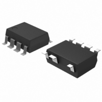
FSD200BM Fairchild Semiconductor, FSD200BM Datasheet

FSD200BM
Specifications of FSD200BM
FSD200BM_NL
Available stocks
Related parts for FSD200BM
FSD200BM Summary of contents
Page 1
... FSD200B 5W 7W FSD210BM 5W 7W FSD200BM 5W 7W Notes: 1. Typical continuous power in a non-ventilated enclosed adapter with sufficient drain pattern as a heat sinker, at 50°C ambient. 2. Maximum practical continuous power in an open frame design with sufficient drain pattern as a heat sinker, at 50°C ambient ...
Page 2
FSD210B, FSD200B Internal Block Diagram Vcc 5 UVLO Frequency Modulation I I DELAY FB 250uA 5uA Vfb 4 Reset V Vcc 5 7V Frequency Modulation I I DELAY FB 250uA 5uA Vfb 4 Reset V 2 Internal Voltage Bias Ref ...
Page 3
Pin Definitions Pin Number Pin Name GND 4 Vfb 5 Vcc 7 Drain 8 Vstr Pin Configuration Pin Function Description Sense FET source terminal on primary side and internal control ground. The feedback voltage pin is the ...
Page 4
FSD210B, FSD200B Absolute Maximum Ratings (Ta=25°C, unless otherwise specified) Characteristic Drain Pin Voltage Vstr Pin Voltage 7DIP Total Power Dissipation Drain Pin Voltage Vstr Pin Voltage 7LSOP Total Power Dissipation Supply Voltage FSD200B Feedback Voltage Range Supply Voltage FSD210B Feedback ...
Page 5
Electrical Characteristics (Ta = 25°C unless otherwise specified) Parameter SENSE FET SECTION Zero-Gate-Voltage Drain Current Drain-Source On-State Resistance Rise Time Fall Time CONTROL SECTION Switching Frequency Switching Frequency Modulation Range Maximum Duty Cycle Minimum Duty Cycle UVLO Threshold Voltage (FSD200B) ...
Page 6
FSD210B, FSD200B Comparison Between FSDH565 and FSD210B Function FSDH565 Soft-Start not applicable Switching Frequency 100KHz Frequency Modulation not applicable Burst Mode Operation not applicable Drain Creepage at 1.02mm Package 6 FSD210B FSD210B Advantages 3ms • Gradually increasing current limit during ...
Page 7
Typical Performance Characteristics (Control Part) (These characteristic graphs are normalized 1.2 1.0 0.8 0.6 0.4 0.2 0.0 - Temperature (℃) Switching Frequency (f 1.2 1.0 0.8 0.6 0.4 0.2 0.0 - ...
Page 8
FSD210B, FSD200B Typical Performance Characteristics 1.2 1.0 0.8 0.6 0.4 0.2 0.0 - Temperature (℃) Vcc Regulation Voltage vs. Ta (for FSD200B) 1.4 1.2 1.0 0.8 0.6 0.4 0.2 0.0 - Temperature (℃) Start ...
Page 9
Functional Description 1. Startup : At startup, the internal high voltage current source supplies the internal bias and charges the external Vcc capacitor as shown in Figure 7. In the case of the FSD210B, when Vcc reaches 8.7V the device ...
Page 10
FSD210B, FSD200B 4. Protection Circuit : The FSD200B/210B have 2 self- protection functions : over load protection (OLP) and thermal shutdown (TSD). Because these protection circuits are fully integrated inside the IC without external compo- nents, the reliability is improved ...
Page 11
Burst operation : In order to minimize the power dissi- pation in standby mode, the FSD200B/210B enter burst mode operation. As the load decreases, the feedback voltage decreases. The device automatically enters burst mode when the feedback voltage drops ...
Page 12
FSD210B, FSD200B Application Tips 1. Methods of Reducing Audible Noise Switching mode power converters have electronic and magnetic components, which generate audible noises when the operating frequency is in the range of 20~20,000 Hz. Even though they operate above 20 ...
Page 13
Typical Application Circuit - 1 Application Output power Cellular Phone Charger Features • High efficiency (>67% at Universal Input) • Low zero load power consumption (<100mW at 240Vac) with FSD210B • Low component count • Enhanced system reliability through various ...
Page 14
FSD210B, FSD200B 2. Transformer Schematic Diagram CORE : EE1616 3. Winding Specification Pin(S → → 2 Insulation : Polyester Tape t = 0.025mm, 2Layers W2 4 → 3 Insulation ...
Page 15
Typical Application Circuit - 2 Application Output power Non-Isolation Buck Features • Non-Isolation Buck converter • Low component count • Enhanced system reliability through various protection functions Key Design Notes • The output voltage(12V) is regulated with resistors R1, R2 ...
Page 16
FSD210B, FSD200B Package Dimensions 16 7-DIP ...
Page 17
Package Dimensions (Continued) 7-LSOP FSD210B, FSD200B 17 ...
Page 18
... FSD200B 7DIP FSD210BM 7LSOP FSD200BM 7LSOP DISCLAIMER FAIRCHILD SEMICONDUCTOR RESERVES THE RIGHT TO MAKE CHANGES WITHOUT FURTHER NOTICE TO ANY PRODUCTS HEREIN TO IMPROVE RELIABILITY, FUNCTION OR DESIGN. FAIRCHILD DOES NOT ASSUME ANY LIABILITY ARISING OUT OF THE APPLICATION OR USE OF ANY PRODUCT OR CIRCUIT DESCRIBED HEREIN; NEITHER DOES IT CONVEY ANY LICENSE UNDER ITS PATENT RIGHTS, NOR THE RIGHTS OF OTHERS ...


