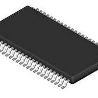
PCA85162T/Q900/1,1 NXP Semiconductors, PCA85162T/Q900/1,1 Datasheet - Page 31

PCA85162T/Q900/1,1
Manufacturer Part Number
PCA85162T/Q900/1,1
Description
IC INTERFACE
Manufacturer
NXP Semiconductors
Datasheet
1.PCA85162TQ90011.pdf
(42 pages)
Specifications of PCA85162T/Q900/1,1
Package / Case
48-TSSOP
Display Type
LCD
Configuration
32 Segment
Interface
I²C
Current - Supply
80µA
Voltage - Supply
1.8 V ~ 5.5 V
Operating Temperature
-40°C ~ 95°C
Mounting Type
Surface Mount
Number Of Digits
16
Number Of Segments
32
Maximum Clock Frequency
4800 Hz
Operating Supply Voltage
1.8 V to 5.5 V
Maximum Power Dissipation
400 mW
Maximum Operating Temperature
+ 95 C
Attached Touch Screen
No
Maximum Supply Current
20 uA
Minimum Operating Temperature
- 40 C
Lead Free Status / RoHS Status
Lead free / RoHS Compliant
Digits Or Characters
-
Lead Free Status / Rohs Status
Details
Other names
568-5119-2
NXP Semiconductors
PCA85162_1
Product data sheet
The SYNC line is provided to maintain the correct synchronization between all cascaded
PCA85162. Synchronization is guaranteed after a power-on reset. The only time that
SYNC is likely to be needed is if synchronization is accidentally lost (e.g. by noise in
adverse electrical environments or by defining a multiplex drive mode when PCA85162
with different SA0 levels are cascaded).
SYNC is organized as an input/output pin. The output selection is realized as an
open-drain driver with an internal pull-up resistor. A PCA85162 asserts the SYNC line at
the onset of its last active backplane signal and monitors the SYNC line at all other times.
If synchronization in the cascade is lost, it is restored by the first PCA85162 to assert
SYNC. The timing relationship between the backplane waveforms and the SYNC signal
for the various drive modes of the PCA85162 are shown in
The contact resistance between the SYNC on each cascaded device must be controlled.
If the resistance is too high, the device is not able to synchronize properly; this is
particularly applicable to chip-on-glass applications. The maximum SYNC contact
resistance allowed for the number of devices in cascade is given in
Fig 22. Cascaded PCA85162 configuration
V
V
V
SS
DD
CONTROLLER
PROCESSOR/
LCD
(1) Is master (OSC connected to V
(2) Is slave (OSC connected to V
MICRO-
MICRO-
HOST
R
≤
All information provided in this document is subject to legal disclaimers.
2C
t
r
b
Rev. 01 — 19 April 2010
DD
SS
).
SYNC
SYNC
).
OSC
SDA
SCL
CLK
OSC
SDA
CLK
SCL
A0
Universal LCD driver for low multiplex rates
A0
A1
PCA85162
PCA85162
V DD
V
A1
DD
A2
(1)
(2)
A2 SA0
V LCD
SA0
V
LCD
V
SS
V
Figure
SS
32 segment drives
32 segment drives
4 backplanes
BP0 to BP3
BP0 to BP3
(open-circuit)
23.
PCA85162
Table
© NXP B.V. 2010. All rights reserved.
19.
LCD PANEL
013aaa058
31 of 42


