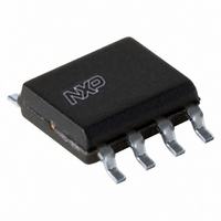
PCA9512AD,112 NXP Semiconductors, PCA9512AD,112 Datasheet - Page 13

PCA9512AD,112
Manufacturer Part Number
PCA9512AD,112
Description
IC LEVSHIFT I2C/SMBUS BUFF 8SOIC
Manufacturer
NXP Semiconductors
Type
I²C-Bus and SMBus Switchr
Specifications of PCA9512AD,112
Package / Case
8-SOIC (0.154", 3.90mm Width)
Applications
Hot-Swap/SMB Buffer
Internal Switch(s)
Yes
Voltage - Supply
2.7 V ~ 5.5 V
Operating Temperature
-40°C ~ 85°C
Mounting Type
Surface Mount
Logic Family
PCA
Maximum Operating Temperature
85 C
Mounting Style
SMD/SMT
Minimum Operating Temperature
- 40 C
Number Of Lines (input / Output)
3 / 3
Logic Type
Bus Buffer
Lead Free Status / RoHS Status
Lead free / RoHS Compliant
Lead Free Status / RoHS Status
Lead free / RoHS Compliant, Lead free / RoHS Compliant
Other names
568-3361-5
935279721112
PCA9512AD
935279721112
PCA9512AD
NXP Semiconductors
Table 5.
V
[1]
[2]
[3]
[4]
[5]
[6]
[7]
[8]
[9]
PCA9512A_PCA9512B
Product data sheet
Symbol
System characteristics
f
t
t
t
t
t
t
t
t
t
t
SCL
BUF
HD;STA
SU;STA
SU;STO
HD;DAT
SU;DAT
LOW
HIGH
f
r
CC
= 2.7 V to 5.5 V; T
This specification applies over the full operating temperature range.
Card side supply voltage.
The enable time is from power-up of V
Idle time is from when SDAn and SCLn are HIGH after enable time has been met.
I
Input pull-up voltage should not exceed power supply voltage in operating mode because the rise time accelerator will clamp the voltage
to the positive supply rail.
The connection circuitry always regulates its output to a higher voltage than its input. The magnitude of this offset voltage as a function
of the pull-up resistor and V
Guaranteed by design, not production tested.
C
trt(pu)
b
= total capacitance of one bus line in pF.
varies with temperature and V
Characteristics
Parameter
SCL clock frequency
bus free time between a
STOP and START condition
hold time (repeated) START
condition
set-up time for a repeated
START condition
set-up time for STOP
condition
data hold time
data set-up time
LOW period of the SCL
clock
HIGH period of the SCL
clock
fall time of both SDA and
SCL signals
rise time of both SDA and
SCL signals
amb
=
−
…continued
CC
40
voltage is shown in
°
C to +85
CC
CC
voltage, as shown in
and V
All information provided in this document is subject to legal disclaimers.
°
C; unless otherwise specified.
Conditions
CC2
Section 11.1 “Typical performance
≥ 2.7 V to when idle or stop time begins.
Rev. 5 — 5 January 2011
Level shifting hot swappable I
Section 11.1 “Typical performance
PCA9512A; PCA9512B
[8][9]
[8][9]
characteristics”.
[8]
[8]
[8]
[8]
[8]
[8]
[8]
[8]
[8]
Min
0
1.3
0.6
0.6
0.6
300
100
1.3
0.6
20 + 0.1 × C
20 + 0.1 × C
characteristics”.
2
C-bus and SMBus bus buffer
b
b
Typ
-
-
-
-
-
-
-
-
-
-
-
© NXP B.V. 2011. All rights reserved.
Max
400
-
-
-
-
-
-
-
-
300
300
13 of 24
Unit
kHz
μs
μs
μs
μs
ns
ns
μs
μs
ns
ns


