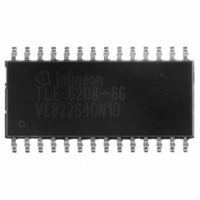
TLE6208-6G Infineon Technologies, TLE6208-6G Datasheet

TLE6208-6G
Specifications of TLE6208-6G
SP000305936
TLE6208-6G
TLE6208-6GINTR
TLE62086GNT
TLE62086GT
TLE62086GXT
Available stocks
Related parts for TLE6208-6G
TLE6208-6G Summary of contents
Page 1
Hex-Half-Bridge / Double Six-Driver 1 Overview 1.1 Features • Six High-Side and six Low-Side-Drivers • Free configurable as switch, halfbridge or H-bridge • Optimized for DC motor management applications • 0.6 A continuous (1 A peak) current per switch R ...
Page 2
Pin Configuration (top view) Figure 1 Data Sheet PG-DSO-28-24 2 TLE 6208-6 G 2007-09-12 ...
Page 3
Pin Definitions and Functions Pin No. Symbol Function 1 OUTL5 Low-Side-Output 5; Power-MOS open drain with internal reverse diode; no internal clamp diode or active zenering; short circuit protected and open load controlled. 2 OUTH5 High-Side-Output 5; Power-MOS open ...
Page 4
Pin Definitions and Functions (cont’d) Pin No. Symbol Function 20, 21, GND Ground 22 CSN Chip-Select-Not input; CSN is an active low input; serial communication is enabled by pulling the CSN terminal low; CSN input should only ...
Page 5
Functional Block Diagram Figure 2 Block Diagram TLE 6208-6 G Data Sheet 5 TLE 6208-6 G 2007-09-12 ...
Page 6
Circuit Description Figure 2 shows a block schematic diagram of the module. There are 6 halfbridge drivers on the right-hand side driver and an LS driver are combined to form a halfbridge driver in each case. The ...
Page 7
When commutating inductive loads, the dissipated power peak can be significantly reduced by activating the transistor located parallel to the internal freewheeling diode. A special, integrated “timer” for power ON/OFF times ensures there is no crossover current at the halfbridge. ...
Page 8
Table 1 Input Data Protocol BIT 15 OVLO on/off 14 Underload SD on/off 13 Overcurrent SD on/off 12 HS-Switch 6 11 LS-Switch 6 10 HS-Switch 5 9 LS-Switch 5 8 HS-Switch 4 7 LS-Switch 4 6 HS-Switch 3 5 LS-Switch ...
Page 9
Table 3 Fault Result Table Fault Diag.-Bit Overcurrent (load) 13 Short circuit to GND 13 (high-side-switch) V Short circuit (low-side-switch) Temperature warning 0 Temperature shut – down (SD) Openload 14 Underload 14 Undervoltage lockout 15 (UVLO) Overvoltage ...
Page 10
Electrical Characteristics 2.1 Absolute Maximum Ratings Parameter Voltages Supply voltage Supply voltage Logic supply voltage Logic input voltages (DI, CLK, CSN, INH) Logic output voltage (DO) Currents Output current (cont.), if Bit13 (OCSD) is set. Output current (cont.), if ...
Page 11
Operating Range Parameter Supply voltage Supply voltage slew rate Logic supply voltage Supply voltage increasing Supply voltage decreasing Logic input voltage (DI, CLK, CSN, INH) SPI clock frequency Junction temperature Thermal Resistances Junction pin Junction ambient Data Sheet Symbol ...
Page 12
Electrical Characteristics < < 4.75 V < S unless otherwise specified Parameter Current Consumption Quiescent current Quiescent current Supply current Logic-Supply current Logic-Supply current Over- and Under-Voltage Lockout UV-Switch-ON voltage UV-Switch-OFF voltage UV-ON/OFF-Hysteresis ...
Page 13
Electrical Characteristics (cont’ < < 4.75 V < S unless otherwise specified Parameter Outputs OUTH1-6 and OUTL1-6 Static Drain-Source-On Resistance Source (High-Side – 0.5 A OUT Sink (Low-Side 0.5 ...
Page 14
Electrical Characteristics (cont’ < < 4.75 V < S unless otherwise specified Parameter Overcurrent Source shutdown threshold Sink shutdown threshold Current limit Shutdown delay time Open Circuit Detection current Delay time Delay Time ...
Page 15
Electrical Characteristics (cont’ < < 4.75 V < S unless otherwise specified Parameter Output Switching Times; Source (high-side) rise-time Source (high-side) fall-time Sink (low-side) fall-time Sink (low-side) rise-time Clamp Diodes Forward Voltage Upper ...
Page 16
Electrical Characteristics (cont’ < < 4.75 V < S unless otherwise specified Parameter SPI-Interface Delay Time from Stand-by to Data In Setup time Logic Inputs DI, CLK and CSN H-input voltage threshold L-input ...
Page 17
Electrical Characteristics (cont’ < < 4.75 V < S unless otherwise specified Parameter Data Input Timing Clock period Clock high time Clock low time Clock low before CSN low CSN setup time CSN ...
Page 18
Electrical Characteristics (cont’ < < 4.75 V < S unless otherwise specified Parameter Thermal Prewarning and Shutdown Thermal prewarning junction temperature Temperature prewarning hysteresis Thermal shutdown junction temperature Thermal switch-on junction temperature Temperature ...
Page 19
Timing Diagrams CSN High to Low & rising edge of CLK enabled. Status information is transfered to Output Shift Register CSN CSN Low to High: Data from Shift-Register is transfered to Output Power Switches CLK 0 1 ...
Page 20
Figure 6 SPI-Input Timing CSN Case 1 ON State I OUT Case 2 OFF State I OUT Figure 7 Turn OFF/ON Time Data Sheet t CSNH t rIN t dOFF t OFF t dON TLE 6208-6 G ...
Page 21
CLK DO ( low to high ) ( high to low ) DO Figure 8 DO Valid Data Delay Time and Valid Time CSN DO DO Figure 9 DO Enable and Disable Time Data Sheet t rIN t rDO t ...
Page 22
Application Figure 10 Application Circuit Data Sheet 22 TLE 6208-6 G 2007-09-12 ...
Page 23
Package Outlines Figure 11 PG-DSO-28-24 (Plastic Dual Small Outline) Green Product (RoHS compliant) To meet the world-wide customer requirements for environmentally friendly products and to be compliant with government regulations the device is available as a green product. Green ...
Page 24
Revision History Version Date Rev. 1.1 2007-09-12 RoHS-compliant version of the TLE 6208-6 G Data Sheet Changes • All pages: Infineon logo updated • Page 1: “added AEC qualified” and “RoHS” logo, “Green Product (RoHS compliant)” and “AEC qualified” statement ...
Page 25
... Infineon Technologies Office. Infineon Technologies components may be used in life-support devices or systems only with the express written approval of Infineon Technologies failure of such components can reasonably be expected to cause the failure of that life-support device or system or to affect the safety or effectiveness of that device or system. Life support devices or systems are intended to be implanted in the human body or to support and/or maintain and sustain and/or protect human life ...


