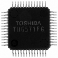
TB6571FG(O,EL) Toshiba, TB6571FG(O,EL) Datasheet - Page 19

TB6571FG(O,EL)
Manufacturer Part Number
TB6571FG(O,EL)
Description
IC DC MOTOR CTRLR BRUSHLSS 52QFP
Manufacturer
Toshiba
Specifications of TB6571FG(O,EL)
Applications
DC Motor Controller, Brushless (BLDC), 3 Phase
Number Of Outputs
1
Voltage - Supply
10 V ~ 28 V
Operating Temperature
-30°C ~ 85°C
Mounting Type
Surface Mount
Package / Case
52-QFP
Mounting Style
SMD/SMT
Lead Free Status / RoHS Status
Lead free / RoHS Compliant
Current - Output
-
Voltage - Load
-
Lead Free Status / Rohs Status
Lead free / RoHS Compliant
Other names
TB6571FGTR
Available stocks
Company
Part Number
Manufacturer
Quantity
Price
Constant voltage circuit
Overcurrent protection circuit
Power supply monitor circuit
Thermal shutdown circuit
The circuit monitors the Vref and Vcc voltages and turns the external power FET off if any of the following
conditions are satisfied:
V
The circuit turns the external output power FET off if the junction temperature TSD (ON) exceeds 160°C.
The thermal shutdown state is terminated once the TB6571FG is placed in the stop or brake state.
(1)
(2)
(3)
CC
• The circuit turns the external output power FET off if the detected voltage is higher than 0.25 V (typ.).
(H) ≤ 9 V, V
It re-activates the FET according to the carrier frequency.
Note that the Idc pin accepts a direct analog comparator input and is highly sensitive. Use C and R,
therefore, for filtering so that output current noise due to chopping does not activate the overcurrent
protection circuit.
Vref1
• The circuit creates 5 V for biasing the internal analog circuit and outputs it from the Vref pin.
V
• The circuit outputs 5 V for biasing the internal logic circuit from the V
Vref2
• The circuit creates 8 V for output FET gate driving and outputs it from the Vref2 pin.
DD
Connect a capacitor (0.1 µF to 1 µF) between the Vref pin and L-GND to prevent oscillation and
absorb noise.
The output load current is 10 mA.
Vref = 5 V (typ.) ± 0.5 V at Io = 10 mA
Connect a capacitor (1 µF recommended) between the V
and absorb noise.
Connect no load to the V
Connect a capacitor (1 µF or larger) between the Vref2 pin and L-GND to prevent oscillation and
absorb noise.
CC
(L) ≤ 8.5 V, Vref1 (H) ≤ 4.5 V, Vref1 (L) ≤ 4.0 V
Idc
V
CC
DD
pin.
19
V
ref
DD
pin and L-GND to prevent oscillation
DD
pin.
TB6571FG
2005-04-15


