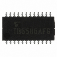
TB6586AFG(O,EL,DRY) Toshiba, TB6586AFG(O,EL,DRY) Datasheet

TB6586AFG(O,EL,DRY)
Specifications of TB6586AFG(O,EL,DRY)
Related parts for TB6586AFG(O,EL,DRY)
TB6586AFG(O,EL,DRY) Summary of contents
Page 1
... TOSHIBA Bi-CMOS Integrated Circuit Silicon Monolithic TB6586FG, TB6586AFG Three-Phase Full-Wave Brushless Motor Controller Features • Upper-phase PWM control • Built-in triangular-wave generator • Support of a bootstrap circuit • Built-in Hall amplifier (support of a Hall element) • Selectable 120°/150° energization • ...
Page 2
Pin Description Pin No. Symbol 1 V Speed control SP 2 HUP U-phase Hall signal input (+) pin 3 HUM U-phase Hall signal input (−) pin 4 HVP V-phase Hall signal input (+) pin 5 HVM V-phase Hall signal input ...
Page 3
Input/Output Equivalent Circuits Pin Description Symbol HUP HUM HVP Positional signal input pin HVM HWP HWM Speed control signal V SP input pin Rotation direction signal input pin CW/CCW L: Forward (CW) H: Reverse (CCW) Reset input RESET L: 150° ...
Page 4
Pin Description Symbol Analog Analog filter 0.5 µs (typ.) Overcurrent protection signal RS input 0.5 V (typ.) or higher, UH, VH and WH pin goes low (released at carrier cycle) 5.0 ± 0.5 V (35 mA) Reference ...
Page 5
Block Diagram V 16 (internal reference CC protection circuit CW/CCW 11 HUP 2 HUM 3 HVP 4 HVM 5 HWP 6 HWM OSC/C 12 Oscillating circuit OSC RESET refout 8 15 5-V ...
Page 6
Absolute Maximum Ratings Characteristic Supply voltage Input voltage Turn-on signal output current Supply voltage Operating temperature Storage temperature Note 1: CW/CCW, RESET Note Note 3: No heatsink Note 4: When mounted on a PCB (50 × 50 ...
Page 7
Electrical Characteristics Characteristic Supply current Output current Input current Input voltage Input sensitivity Hall element input Common mode Input hysteresis Input hysteresis voltage Input delay Output voltage Output leakage current Electrical current detector Lead angle correction V monitor CC (Unless ...
Page 8
Characteristic PWM oscillator frequency (carrier frequency) Output duty (max) Note: Pre-shipment testing is not performed. Test Symbol Test Condition Circuit OSC/C = 560 pF, F OSC/R = 6.2 kΩ C (20) OSC/C = 470 pF, (18) ...
Page 9
Functional Description 1. Basic operation At startup, the motor runs at 120° energization. When the position detection signal reaches a revolution count higher, the rotor position is extrapolated from the position detection signal and ...
Page 10
If the V input current is 2.1 V < WH) will perform 120° energization at a PWM that complies with the V VL, WL) will operate at 120° energization, performing refresh operation based on the OFF timing. ...
Page 11
Setting the carrier frequency This function involves setting the triangular wave cycle (carrier cycle) necessary for generating PWM signals. Carrier frequency osc = 5 MHz, then f Example osc = 4 MHz, then ...
Page 12
Protecting input pin (1) Overcurrent protection (Pin RS) When the DC link current exceeds the internal reference voltage, this pin performs gate block protection. Overcurrent protection is restored for each carrier frequency. The pin is equipped with a filter ...
Page 13
Low GND) Timing Chart (Normal Hall input) HUM HUP HVM HVP HWM HWP 0 < Hall < (120° energization < Hall (120° energization: RESET = ...
Page 14
High GND) Timing Chart (Normal Hall input) HUM HUP HVM HVP HWM HWP Reverse detection (120° energization When CW/CCW = Low and a reverse Hall signal is input, ...
Page 15
High GND) Timing Chart (Reverse Hall input) HUM HUP HVM HVP HWM HWP 0 < Hall < (120° energization < Hall (120° energization: RESET = ...
Page 16
Low GND) Timing Chart (Reverse Hall input) HUM HUP HVM HVP HWM HWP Reverse detection (120° energization When CW/CCW = Low and a reverse Hall signal is input, ...
Page 17
Example Application Circuit = 6.5~16 refout CW/CCW V refout Hall element C MCU R Note: Utmost care is necessary in the design of the output faults due to improper grounding short-circuiting between ...
Page 18
Package Dimensions Weight: 0.27 g (typ.) 18 TB6586FG/AFG 2007-08-03 ...
Page 19
... Application Circuits The application circuits shown in this document are provided for reference purposes only. Thorough evaluation is required, especially at the mass production design stage. Toshiba does not grant any license to any industrial property rights by providing these examples of application circuits. 5. Test Circuits Components in the test circuits are used only to obtain and confirm the device characteristics. These components and circuits are not guaranteed to prevent malfunction or failure from occurring in the application equipment ...
Page 20
... The information contained herein is presented only as a guide for the applications of our products. No responsibility is assumed by TOSHIBA for any infringements of patents or other rights of the third parties which may result from its use. No license is granted by implication or otherwise under any patents or other rights of TOSHIBA or the third parties ...


