MCZ33689DEW Freescale Semiconductor, MCZ33689DEW Datasheet - Page 13
MCZ33689DEW
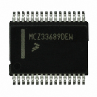
Manufacturer Part Number
MCZ33689DEW
Description
IC SYSTEM BASIS CHIP LIN 32-SOIC
Manufacturer
Freescale Semiconductor
Datasheet
1.MC33689DDWBR2.pdf
(31 pages)
Specifications of MCZ33689DEW
Applications
Automotive
Current - Supply
5mA
Voltage - Supply
5.5 V ~ 18 V
Operating Temperature
-40°C ~ 125°C
Mounting Type
Surface Mount
Package / Case
32-SOIC (7.5mm Width)
Lead Free Status / RoHS Status
Lead free / RoHS Compliant
Available stocks
Company
Part Number
Manufacturer
Quantity
Price

Part Number:
MCZ33689DEW
Manufacturer:
FREESCALE
Quantity:
20 000


Table 4. Dynamic Electrical Characteristics (continued)
Typical values noted reflect the approximate parameter means at T
Analog Integrated Circuit Device Data
Freescale Semiconductor
CURRENT SENSE OPERATIONAL AMPLIFIER
L1 AND L2 INPUT PINS
STATE MACHINE TIMING
Notes
Supply Voltage Rejection Ratio
Common Mode Rejection Ratio
Gain Bandwidth
Output Slew Rate
Phase Margin
Open Loop Gain
Wake-Up Filter Time
Delay Between
and Stop Mode Activation
Interrupt Low-Level Duration
Internal Oscillator Frequency Accuracy (All Modes, for Information Only)
Normal Request Mode Time-Out (Normal Request Mode)
Delay Between SPI Command and HS1 or HS2 Turn On
Delay Between SPI Command and HS1 or HS2 Turn Off
Delay Between SPI Command and HS3 Turn On
Delay Between SPI Command and HS3 Turn Off
Delay Between Normal Request and Normal Mode After a Watchdog Trigger
Command (Normal Request Mode)
Delay Between
Delay Between Interrupt Pulse in Stop Mode After Wake-Up and First
Accepted SPI Command
Minimum Time Between Rising and Falling Edge on the
16.
17.
18.
19.
Characteristics noted under conditions 5.5 V ≤ V
Minimum Watchdog Period
No Watchdog Selected
Maximum Watchdog Period
Normal Mode, V
Normal Mode, V
Normal Mode, V
Normal Mode, V
Normal Request Mode, VDD ON and
First Accepted SPI Command
Parameter guaranteed by design; however, it is not production tested.
When IN input is set to HIGH, delay starts at falling edge of clock cycle #8 of the SPI command and start of device activation/deactivation.
30 mA load on high-side switches. Excluding rise or fall time due to external load.
When IN is used to control the high-side switches, delays are measured between IN and HS1 or HS2 ON / OFF. 30 mA load on high-side
switches, excluding rise or fall time due to external load.
Delay between turn on or turn off command and HS ON or HS OFF, excluding rise or fall time due to external load.
CS
CS
(16)
(16)
LOW-to-HIGH Transition (at End of SPI Stop Command)
SUP
SUP
SUP
SUP
Wake-Up (
(16)
> 9.0 V, V
> 9.0 V, V
> 9.0 V, V
> 9.0 V, V
(16)
CS
Characteristic
(16)
(16)
LOW to HIGH) in Stop Mode and:
HS
HS
HS
HS
(16)
≥ 0.2 V
≤ 0.8 V
≥ 0.2 V
≤ 0.8 V
RST
VS2
VS2
VS2
VS2
HIGH
(17)
(17)
,
,
(19)
(19)
SUP
CS
(17)
(17)
≤ 18 V, - 40°C ≤ T
,
,
(18)
(18)
A
= 25°C under nominal conditions unless otherwise noted.
A
t
t
Symbol
t
t
t
t
NRTOUT
SHSOFF
t
PHMO
SHSOFF
t
t
S1STSPI
SHSON
t
SHSON
SNR2N
CMR
t
WUSPI
SVR
GBP
OLG
f
WUCS
t
≤ 125°C, GND = 0.0 V unless otherwise noted.
STOP
t
WUF
OSC
SR
2
INT
CS
DYNAMIC ELECTRICAL CHARACTERISTICS
Min
- 35
1.0
0.5
8.0
1.4
6.0
7.0
7.0
60
70
40
12
97
15
90
30
15
—
—
—
—
—
ELECTRICAL CHARACTERISTICS
Typ
150
85
20
10
15
40
—
—
—
—
—
—
—
—
—
—
—
—
—
—
—
—
Max
205
N/A
N/A
5.0
38
30
50
13
35
20
20
20
20
30
80
—
—
—
—
—
—
—
Unit
MHz
V/µs
deg.
ms
dB
dB
dB
µs
µs
µs
µs
µs
µs
µs
µs
µs
µs
µs
%
33689
13
Related parts for MCZ33689DEW
Image
Part Number
Description
Manufacturer
Datasheet
Request
R

Part Number:
Description:
Manufacturer:
Freescale Semiconductor, Inc
Datasheet:
Part Number:
Description:
Manufacturer:
Freescale Semiconductor, Inc
Datasheet:
Part Number:
Description:
Manufacturer:
Freescale Semiconductor, Inc
Datasheet:
Part Number:
Description:
Manufacturer:
Freescale Semiconductor, Inc
Datasheet:
Part Number:
Description:
Manufacturer:
Freescale Semiconductor, Inc
Datasheet:
Part Number:
Description:
Manufacturer:
Freescale Semiconductor, Inc
Datasheet:
Part Number:
Description:
Manufacturer:
Freescale Semiconductor, Inc
Datasheet:
Part Number:
Description:
Manufacturer:
Freescale Semiconductor, Inc
Datasheet:
Part Number:
Description:
Manufacturer:
Freescale Semiconductor, Inc
Datasheet:
Part Number:
Description:
Manufacturer:
Freescale Semiconductor, Inc
Datasheet:
Part Number:
Description:
Manufacturer:
Freescale Semiconductor, Inc
Datasheet:
Part Number:
Description:
Manufacturer:
Freescale Semiconductor, Inc
Datasheet:
Part Number:
Description:
Manufacturer:
Freescale Semiconductor, Inc
Datasheet:
Part Number:
Description:
Manufacturer:
Freescale Semiconductor, Inc
Datasheet:
Part Number:
Description:
Manufacturer:
Freescale Semiconductor, Inc
Datasheet: