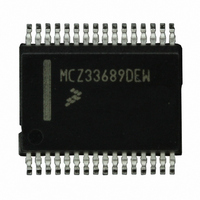
MCZ33689DEW Freescale Semiconductor, MCZ33689DEW Datasheet - Page 25

MCZ33689DEW
Manufacturer Part Number
MCZ33689DEW
Description
IC SYSTEM BASIS CHIP LIN 32-SOIC
Manufacturer
Freescale Semiconductor
Datasheet
1.MC33689DDWBR2.pdf
(31 pages)
Specifications of MCZ33689DEW
Applications
Automotive
Current - Supply
5mA
Voltage - Supply
5.5 V ~ 18 V
Operating Temperature
-40°C ~ 125°C
Mounting Type
Surface Mount
Package / Case
32-SOIC (7.5mm Width)
Lead Free Status / RoHS Status
Lead free / RoHS Compliant
Available stocks
Company
Part Number
Manufacturer
Quantity
Price
Part Number:
MCZ33689DEW
Manufacturer:
FREESCALE
Quantity:
20 000
LIN-PU — LIN Pullup Enable Bit
Stop modes in accordance with
LIN-PU bit.
HS3: HS1 — High-Side H3 : HS1 Enable Bits
Table
must be connected to the VDD pin.
MODE2 and MODE1 — Mode Section Bits
modes in accordance with
Analog Integrated Circuit Device Data
Freescale Semiconductor
Table 4. LIN Pullup Termination Control Bit (D5)
LIN-PU
Table 6. Mode Control Bits (D1 and D0)
Notes
MODE2
This bit controls the LIN pullup resistor during Sleep and
These bits enable the HS3 : HS1 bits in accordance with
Note If no PWM on HS1 and HS2 is required, the IN pin
The MODE2 and MODE1 bits control the 33689 operating
3.
4.
0
1
0
0
1
1
5. Reset clears the HSx bit.
Special SPI command and sequence is implemented in
order to avoid going into Sleep or Stop mode with a single
8-bit SPI command. Refer to
When a logic [0] is written to MODE1 bit while MODE2 bit
is written as a logic [1]. After the SPI command is
completed, MODE1 bit is set to logic [1] and the 33689
stays in Normal mode. In order to set the 33689 in Sleep
mode, both MODE1 and MODE2 bits must be written in
the same 8-bit SPI command. The Watchdog clear on
Normal Request mode (150 ms) has no window.
30 kΩ pullup disconnected in Sleep and Stop mode
MODE1
30 kΩ pullup connected in Sleep and Stop mode
0
1
0
1
Table 5. High-Side Switches Control Bits (D4, D3, and D2)
HS3
0
1
Normal mode + Watchdog clear
Table
Description
Description
HS3 OFF
HS3 ON
Table
6.
Sleep mode
Tables 7
Normal mode
Description
Stop mode
4. Reset clears the
and 8.
(3)
HS2
0
1
(4)
HS2 ON (if IN = 1)
Description
HS2 OFF
these modes are not affected by noise issue during SPI
transmission, the Sleep / Stop commands require two SPI
transmissions.
Sleep Mode Sequence The Sleep command, as shown in
Table
Table 7. Sleep Command Bits
Stop Mode Sequence The Stop command, as shown in
Table
Table 8. Stop Command Bits
LINSL2 LINSL1 LIN-PU
LINSL2 LINSL1 LIN-PU
x = Don’t care.
x = Don’t care.
To safely enter Sleep or Stop mode and to ensure that
1
1
7, must be sent twice.
8, must be sent twice.
1
1
HS1
0
1
x
x
HS3
HS3
0
0
HS1 ON (if IN = 1)
FUNCTIONAL DEVICE OPERATION
Description
HS1 OFF
HS2
HS2
FUNCTIONAL DESCRIPTION
0
0
HS1
HS1
0
0
MODE2 MODE1
MODE2 MODE1
0
0
33689
0
1
25


