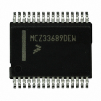
MCZ33689DEW Freescale Semiconductor, MCZ33689DEW Datasheet - Page 23

MCZ33689DEW
Manufacturer Part Number
MCZ33689DEW
Description
IC SYSTEM BASIS CHIP LIN 32-SOIC
Manufacturer
Freescale Semiconductor
Datasheet
1.MC33689DDWBR2.pdf
(31 pages)
Specifications of MCZ33689DEW
Applications
Automotive
Current - Supply
5mA
Voltage - Supply
5.5 V ~ 18 V
Operating Temperature
-40°C ~ 125°C
Mounting Type
Surface Mount
Package / Case
32-SOIC (7.5mm Width)
Lead Free Status / RoHS Status
Lead free / RoHS Compliant
Available stocks
Company
Part Number
Manufacturer
Quantity
Price
Part Number:
MCZ33689DEW
Manufacturer:
FREESCALE
Quantity:
20 000
NORMAL MODE
compatible with the LIN protocol specification. The LIN bus
can transmit and receive information. The V
ON and the watchdog function can be enabled.
SLEEP AND STOP MODE
these modes are not inadvertently entered due to noise
issues during SPI transmission, a dedicated sequence must
be sent twice: data with the bits controlling the LIN bus and
the device mode.
Table 1. Operational Modes and Associated Functions
Analog Integrated Circuit Device Data
Freescale Semiconductor
Device Mode
In Normal Mode, the 33689 has slew rate and timing
To safely enter Sleep or Stop modes and to ensure that
Request
Normal
Normal
Reset
Sleep
Stop
(Limited current
to enter Normal
after Wake-Up
VDD Voltage
(Set to 5.0 V
Regulator
VDD: OFF
capability)
VDD: ON
VDD: ON
VDD: ON
VDD: ON
Request)
LIN and state
LIN and state
Capabilities
L1:L2 inputs
L1:L2 inputs
change on
change on
Wake-Up
N/A
N/A
N/A
DD
regulator is
above threshold)
Go to HIGH after
Normal Request
Watchdog fail (if
LOW for 1.0 ms
Normally HIGH.
HIGH (if VDD
Active LOW if
Active LOW if
Active LOW if
Wake-Up and
undervoltage
occurs and if
undervoltage
undervoltage
RST
specification
typical, then
VDD within
occurs or if
Watchdog
Watchdog
timeout (if
enabled)
enabled)
occurs
HIGH.
HIGH.
LOW.
VDD
VDD
VDD
Output
150 ms timeout
Entering Sleep Mode
D5 = 0 or 1, D1 = 0, and D0 = 0) 11x00000 must be sent.
Entering Stop Mode
D5 = 0 or 1, D1 = 0, and D0 = 1) 11x00001 must be sent.
command. Register bit D5 must be set accordingly.
if Watchdog
Watchdog if
Watchdog
Function
Disabled
Disabled
Disabled
enabled
Window
enabled
First and second SPI commands (with bit D6 = 1, D7 = 1,
First and second SPI commands (with bit D6 = 1, D7 = 1,
Sleep or Stop modes are entered after the second SPI
HS1, HS2, HS3
ON or OFF
ON or OFF
OFF
OFF
OFF
FUNCTIONAL DEVICE OPERATION
Recessive state
Recessive state
Recessive only
LIN Interface
Transmit and
Transmit and
with Wake
with Wake
capability
capability
FUNCTIONAL DESCRIPTION
receive
receive
Operational
Not active
Not active
Not active
Not active
Amplifier
Active
33689
23


