MCZ33689DEW Freescale Semiconductor, MCZ33689DEW Datasheet - Page 24
MCZ33689DEW
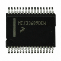
Manufacturer Part Number
MCZ33689DEW
Description
IC SYSTEM BASIS CHIP LIN 32-SOIC
Manufacturer
Freescale Semiconductor
Datasheet
1.MC33689DDWBR2.pdf
(31 pages)
Specifications of MCZ33689DEW
Applications
Automotive
Current - Supply
5mA
Voltage - Supply
5.5 V ~ 18 V
Operating Temperature
-40°C ~ 125°C
Mounting Type
Surface Mount
Package / Case
32-SOIC (7.5mm Width)
Lead Free Status / RoHS Status
Lead free / RoHS Compliant
Available stocks
Company
Part Number
Manufacturer
Quantity
Price

Part Number:
MCZ33689DEW
Manufacturer:
FREESCALE
Quantity:
20 000


SPI INTERFACE AND REGISTER DESCRIPTION
sent as bytes. The MSB, D7, is sent first. The minimum time
between two rising edges on the
showing reset values and reset conditions.
SPI Register: Write Control Bits
LINSL2 and LINSL1 — LIN Baud Rate and Low-Power
Mode Pre-Selection Bits
power mode in accordance with
LINSL2 : 1 bits.
24
33689
FUNCTIONAL DESCRIPTION
FUNCTIONAL DEVICE OPERATION
Table 2. SPI Register Overview
Notes
As shown in
The following tables describe the SPI Register bits,
These bits select the LIN slew rate and requested low-
Read / Write
Information
Write Reset
Write Reset
Condition
1.
2.
Value
Write
Read
D7 signals interrupt source. After interrupt occurs, if D7 is a logic [1] D6 : D0 indicate the interrupt source. If D7 is a logic [0] no interrupt
has occurred and D6 : D0 report real-time status.
The first SPI read after a 33689 reset returns the BATFAIL status flag bit D4.
Figure
INTSRC
LINSL2
RESET
POR,
MSB
2, the SPI is an 8-bit SPI. All data is
D7
0
(1)
MISO
Table
CS
LINWU or
LINFAIL
LINSL1
RESET
POR,
pin is 15 µs.
D6
0
3. Reset clears the
Bit7
D7
LOGIC COMMANDS AND REGISTERS
Figure 2. Data Format Description
Bit6
D6
LIN-PU
VSOV
POR
D5
0
Bit5
D5
D4
Bit4
BATFAIL
VSUV or
RESET
POR,
HS3
D4
0
reports the state of the 33689 at time of a
transition. The status flags are latched at a
transition.
Bit3
D3
Table 3. LIN Slew Rate Control and Device Low Power
LINSL2
(2)
During an SPI data communication, the state of MISO
Bits
0
0
1
1
Bit2
D2
Mode Pre-Selection Bits (D7 and D6)
RESET
VDDT
POR,
LINSL1
HS2
D3
0
0
1
0
1
Bit1
D1
LIN slew rate fast (for program download,
Bit0
Analog Integrated Circuit Device Data
D0
Low power mode (Sleep or Stop mode)
RESET
HSST
request, no change in LIN slew rate
POR,
HS1
D2
0
baud rate up to 100 kbps)
(baud rate up to 20 kbps)
(baud rate up to 10 kbps)
MOSI
LIN slew rate normal
LIN slew rate slow
Freescale Semiconductor
Description
MODE2
D1
L2
—
—
CS
CS
HIGH-to-LOW
HIGH-to-LOW
MODE1
LSB
D0
L1
—
—
Related parts for MCZ33689DEW
Image
Part Number
Description
Manufacturer
Datasheet
Request
R

Part Number:
Description:
Manufacturer:
Freescale Semiconductor, Inc
Datasheet:
Part Number:
Description:
Manufacturer:
Freescale Semiconductor, Inc
Datasheet:
Part Number:
Description:
Manufacturer:
Freescale Semiconductor, Inc
Datasheet:
Part Number:
Description:
Manufacturer:
Freescale Semiconductor, Inc
Datasheet:
Part Number:
Description:
Manufacturer:
Freescale Semiconductor, Inc
Datasheet:
Part Number:
Description:
Manufacturer:
Freescale Semiconductor, Inc
Datasheet:
Part Number:
Description:
Manufacturer:
Freescale Semiconductor, Inc
Datasheet:
Part Number:
Description:
Manufacturer:
Freescale Semiconductor, Inc
Datasheet:
Part Number:
Description:
Manufacturer:
Freescale Semiconductor, Inc
Datasheet:
Part Number:
Description:
Manufacturer:
Freescale Semiconductor, Inc
Datasheet:
Part Number:
Description:
Manufacturer:
Freescale Semiconductor, Inc
Datasheet:
Part Number:
Description:
Manufacturer:
Freescale Semiconductor, Inc
Datasheet:
Part Number:
Description:
Manufacturer:
Freescale Semiconductor, Inc
Datasheet:
Part Number:
Description:
Manufacturer:
Freescale Semiconductor, Inc
Datasheet:
Part Number:
Description:
Manufacturer:
Freescale Semiconductor, Inc
Datasheet: