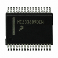
MCZ33689DEW Freescale Semiconductor, MCZ33689DEW Datasheet - Page 15

MCZ33689DEW
Manufacturer Part Number
MCZ33689DEW
Description
IC SYSTEM BASIS CHIP LIN 32-SOIC
Manufacturer
Freescale Semiconductor
Datasheet
1.MC33689DDWBR2.pdf
(31 pages)
Specifications of MCZ33689DEW
Applications
Automotive
Current - Supply
5mA
Voltage - Supply
5.5 V ~ 18 V
Operating Temperature
-40°C ~ 125°C
Mounting Type
Surface Mount
Package / Case
32-SOIC (7.5mm Width)
Lead Free Status / RoHS Status
Lead free / RoHS Compliant
Available stocks
Company
Part Number
Manufacturer
Quantity
Price
Part Number:
MCZ33689DEW
Manufacturer:
FREESCALE
Quantity:
20 000
Table 4. Dynamic Electrical Characteristics (continued)
Typical values noted reflect the approximate parameter means at T
Analog Integrated Circuit Device Data
Freescale Semiconductor
LIN PHYSICAL LAYER: RECEIVER CHARACTERISTICS AND WAKE-UP TIMINGS
Notes
Propagation Delay LIN to RXD
Bus Wake-Up Deglitcher (Sleep and Stop Modes)
Bus Wake-Up Event Reported
24.
25.
26.
27.
Characteristics noted under conditions 5.5 V ≤ V
Dominant State (LIN LOW to RXD LOW)
Recessive State (LIN HIGH to RXD HIGH)
Symmetry (
From Sleep Mode
From Stop Mode
Measured between LIN signal threshold V
See
t
connected to the regulator. The delay is measured between the V
V
rising edge of the LIN bus and the falling edge of the
t
WU
WU
DD
Figures 9
is typically 2 internal clock cycles after a LIN rising edge is detected. In Sleep Mode, the measurement is done without a capacitor
rise time is strongly dependent upon the decoupling capacitor at V
is typically 2 internal clock cycles after a LIN rising edge is detected. In Stop Mode, the delay is measured between the V
t
RDOM
(27)
and 10, page 18.
(26)
-
t
RREC
)
Characteristic
(24)
INL
(25)
or V
SUP
INH
INT
and 50% of RXD signal.
≤ 18 V, - 40°C ≤ T
pin. See
SUP
Figure
A
= 25°C under nominal conditions unless otherwise noted.
/2 rising edge of the LIN bus and when V
DD
10, page 18.
A
t
Symbol
pin. See
PROPWL
t
t
t
RDOM
RSYM
RREC
≤ 125°C, GND = 0.0 V unless otherwise noted.
t
t
WU
WU
Figure
DYNAMIC ELECTRICAL CHARACTERISTICS
- 2.0
Min
30
—
—
—
—
9, page 18.
ELECTRICAL CHARACTERISTICS
Typ
3.0
3.0
70
30
20
—
DD
reaches 3.0 V. The
Max
6.0
6.0
2.0
90
—
—
SUP
Unit
µs
µs
µs
33689
/2
15


