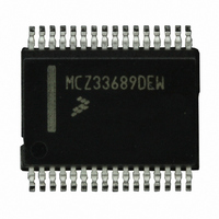
MCZ33689DEW Freescale Semiconductor, MCZ33689DEW Datasheet - Page 19

MCZ33689DEW
Manufacturer Part Number
MCZ33689DEW
Description
IC SYSTEM BASIS CHIP LIN 32-SOIC
Manufacturer
Freescale Semiconductor
Datasheet
1.MC33689DDWBR2.pdf
(31 pages)
Specifications of MCZ33689DEW
Applications
Automotive
Current - Supply
5mA
Voltage - Supply
5.5 V ~ 18 V
Operating Temperature
-40°C ~ 125°C
Mounting Type
Surface Mount
Package / Case
32-SOIC (7.5mm Width)
Lead Free Status / RoHS Status
Lead free / RoHS Compliant
Available stocks
Company
Part Number
Manufacturer
Quantity
Price
Part Number:
MCZ33689DEW
Manufacturer:
FREESCALE
Quantity:
20 000
many functions found in standard microcontroller-based
systems; e.g., power management, communication interface,
system protection, and diagnostics.
functions with a LIN transceiver for slave node applications.
The 33689 has a 5.0 V, 50 mA regulator with undervoltage
reset, output current limiting, overtemperature pre-warning,
and thermal shutdown. An externally selectable timing
Window Watchdog is also included.
LEVEL 1 AND LEVEL 2 INPUT PINS
(L1 AND L2)
wake up the 33689 from Sleep or Stop mode. During Normal
mode, the state of these pins can be read through the SPI
Register. (Refer to the section entitled
Register Description on page 24
Register.)
HIGH-SIDE DRIVER OUTPUT PINS 1 AND 2 (HS1
AND HS2)
as relays or lamps. They are protected against overcurrent
and overtemperature and include internal clamp circuitry for
inductive load protection. Switch control is done through
selecting the correct bit in the SPI Register. HS1 and HS2
can be PWM-ed if required through the IN input pin. The
internal circuitry that drives both high-side switches is an
AND function between the SPI bit HS1 (or HS2) and the IN
input pin.
connected to the VDD pin.
HIGH-SIDE DRIVER OUTPUT PIN 3 (HS3)
Hall sensors, or switch pullup resistors. Control is done
through the SPI Register only.
against overcurrent and short circuit conditions. It is also
protected against overtemperature.
VOLTAGE SUPPLY PINS 1 AND 2
(VS1 AND VS2)
source through the VS1 and VS2 pins. An external diode is
required to protect against negative transients and reverse
Analog Integrated Circuit Device Data
Freescale Semiconductor
A System Basis Chip (SBC) is a monolithic IC combining
The 33689 is a SPI-controlled SBC combining many
These pins are used to sense external switches and to
These two high-side switches are able to drive loads such
If no PWM control is required, the IN pin must be
This high-side switch can be used to drive small lamps,
No direct PWM control is possible on this pin.
This high-side switch features current limit to protect it
The 33689 is supplied from a battery line or other supply
for information on the SPI
SPI Interface and
FUNCTIONAL DESCRIPTION
FUNCTIONAL PIN DESCRIPTION
INTRODUCTION
when high data rates are warranted. A single 50 mA and two
150 mA fully protected high-side switches with output
clamping are available for switching inductive or resistive
loads. The 150 mA switches are PWM capable.
or provide external wake-up. An internal current sense
operational amplifier is available for load current monitoring.
battery. The 33689 can operate from 4.5 V and under the
jump start condition at 27 V DC. Device functionality is
guaranteed down to 4.5 V at VS1 and VS2 pins. These pins
sustain standard automotive voltage conditions such as load
dump at 40 V.
LIN BUS PIN (LIN)
receiver. It is suited for automotive bus systems and is based
on the LIN bus specification.
VOLTAGE SOURCE PIN (VDD)
current sense operational amplifier.
CURRENT SENSE OPERATIONAL AMPLIFIER
PINS (E+, E
operational amplifier.
• The E+ and the E- input pins are the non-inverting and
• The OUT pin is the output pin of the current sense
• The VCC pin is the + 5.0 V single-supply connection for the
Normal mode only.
WATCHDOG CONFIGURATION PIN (
watchdog. A resistor is connected to this pin. The resistor
value defines the watchdog period. If the pin is left open, the
watchdog period is fixed to its default value (150 ms typical).
If no watchdog function is required, the
connected to GND.
The LIN transceiver has waveshaping that can be disabled
Two high-voltage inputs can be used to monitor switches
The LIN pin represents the single-wire bus transmitter and
The VDD pin is the 5.0 V supply pin for the MCU and the
These are the pins of the single-supply current sense
inverting inputs of the current sense operational amplifier,
respectively.
operational amplifier.
current sense operational amplifier.
The current sense operational amplifier is enabled in
The
WDC
pin is the configuration pin for the internal
-
, VCC, AND OUT)
FUNCTIONAL DESCRIPTION
WDC
WDC
INTRODUCTION
pin must be
)
33689
19


