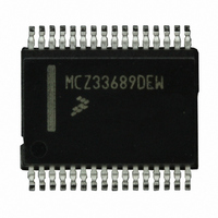
MCZ33689DEW Freescale Semiconductor, MCZ33689DEW Datasheet - Page 20

MCZ33689DEW
Manufacturer Part Number
MCZ33689DEW
Description
IC SYSTEM BASIS CHIP LIN 32-SOIC
Manufacturer
Freescale Semiconductor
Datasheet
1.MC33689DDWBR2.pdf
(31 pages)
Specifications of MCZ33689DEW
Applications
Automotive
Current - Supply
5mA
Voltage - Supply
5.5 V ~ 18 V
Operating Temperature
-40°C ~ 125°C
Mounting Type
Surface Mount
Package / Case
32-SOIC (7.5mm Width)
Lead Free Status / RoHS Status
Lead free / RoHS Compliant
Available stocks
Company
Part Number
Manufacturer
Quantity
Price
Part Number:
MCZ33689DEW
Manufacturer:
FREESCALE
Quantity:
20 000
RESET OUTPUT PIN (
output pin.
PWM INPUT CONTROL PIN (IN)
HS2 high-side switches.
SERIAL DATA CLOCK PIN (SCLK)
changes on the negative transition of the SCLK. MOSI is
sampled on the positive edge of the SCLK.
MASTER OUT SLAVE IN PIN (MOSI)
input is sampled on the positive edge of SCLK.
MASTER IN SLAVE OUT PIN (MISO)
on this output pin changes on the negative edge of the SCLK.
When
CHIP SELECT PIN (
this signal is high, SPI signals are ignored. Asserting this pin
LOW starts an SPI transaction. The transaction is completed
when this signal returns HIGH.
INTERRUPT OUTPUT PIN (
Interrupt pulses are generated for:
20
33689
FUNCTIONAL DESCRIPTION
FUNCTIONAL PIN DESCRIPTION
The
The IN pin is the external PWM control pin for the HS1 and
The SCLK pin is the SPI clock input pin. MISO data
The MOSI pin receives SPI data from the MCU. This data
The MISO pin sends data to an SPI-enabled MCU. Data
The
The
CS
RST
CS
INT
is HIGH, this pin enters the high-impedance state.
pin is the chip select input pin for SPI use. When
pin is used to report 33689 faults to the MCU.
pin is the 5.0 V regulator and Watchdog reset
CS
RST
)
)
INT
)
• Voltage regulator temperature pre-warning
• HS1, HS2, or HS3 thermal shutdown
• VS1 or VS2 overvoltage (20 V typical)
• VS1 or VS2 undervoltage (6.0 V typical)
operation is performed bit D7 in the SPI Register will be set
to logic [1] and bits D6 : D0 will report the interrupt source.
in order to signal to the MCU that a wake-up event from the
L1, L2, or LIN bus pin has occurred.
RECEIVER OUTPUT PIN (RXD)
reports the state of the bus voltage (RXD LOW when LIN bus
is dominant, RXD HIGH when LIN bus is recessive).
TRANSMITTER INPUT PIN (TXD)
and controls the state of the bus output (dominant when TXD
is LOW, recessive when TXD is HIGH).
GROUND PINS (GND, TGND, AND AGND)
• The GND pin is the electrical ground pin for the device.
• The AGND is the analog ground pin for the voltage
• The four TGND pins are the thermal ground pins for the
must be connected together to a ground external to the
33689.
If an interrupt is generated, then when the next SPI read
In cases of wake-up from the Stop mode,
The RXD pin is the receiver output of the LIN interface and
The TXD pin is the transmitter input of the LIN interface
The 33689 has three different types of ground pins.
regulator and current sense operational amplifier.
device.
Important The GND, the AGND, and the four TGND pins
Analog Integrated Circuit Device Data
Freescale Semiconductor
INT
is set LOW


