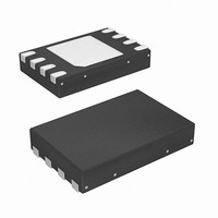
SE97BTP,547 NXP Semiconductors, SE97BTP,547 Datasheet - Page 16

SE97BTP,547
Manufacturer Part Number
SE97BTP,547
Description
IC TEMP SENSOR DIMM 8HWSON
Manufacturer
NXP Semiconductors
Datasheet
1.SE97BTP547.pdf
(53 pages)
Specifications of SE97BTP,547
Package / Case
8-WSON (Exposed Pad), 8-HWSON
Function
Temp Monitoring System (Sensor)
Topology
ADC (Sigma Delta), Comparator, Register Bank
Sensor Type
Internal
Sensing Temperature
-40°C ~ 125°C
Output Type
I²C™/SMBus™
Output Alarm
Yes
Output Fan
Yes
Voltage - Supply
3 V ~ 3.6 V
Operating Temperature
-40°C ~ 125°C
Mounting Type
Surface Mount
Temperature Threshold
+ 150 C
Full Temp Accuracy
2 C
Digital Output - Bus Interface
I2C
Digital Output - Number Of Bits
11 bit
Supply Voltage (max)
3.6 V
Supply Voltage (min)
3 V
Description/function
Temperature Sensor
Maximum Operating Temperature
+ 125 C
Minimum Operating Temperature
- 40 C
Lead Free Status / RoHS Status
Lead free / RoHS Compliant
Lead Free Status / RoHS Status
Lead free / RoHS Compliant, Lead free / RoHS Compliant
Other names
568-5055-2
NXP Semiconductors
SE97B_1
Product data sheet
Fig 11. Byte Write timing
Fig 12. Page Write timing
SDA
SDA
7.10.1.1 Byte Write
7.10.1.2 Page Write
7.10.1 Write operations
START condition
START condition
S
S
1
1
slave address (memory)
slave address (memory)
0
0
In Byte Write mode the master creates a START condition and then broadcasts the slave
address, byte address, and data to be written. The slave acknowledges all 3 bytes by
pulling down the SDA line during the ninth clock cycle following each byte. The master
creates a STOP condition after the last ACK from the slave, which then starts the internal
write operation (see
request from the master.
The SE97B contains 256 bytes of data, arranged in 16 pages of 16 bytes each. The page
is selected by the four Most Significant Bits (MSB) of the address byte presented to the
device after the slave address, while the four Least Significant Bits (LSB) point to the byte
within the page. By loading more than one data byte into the device, up to an entire page
can be written in one write cycle (see
increment automatically after each data byte. If the master transmits more than
16 data bytes, then earlier bytes will be overwritten by later bytes in a wrap-around
fashion within the selected page. The internal write cycle is started following the STOP
condition created by the master.
1
1
0
0
A2 A1 A0
A2 A1 A0
R/W acknowledge
R/W acknowledge
0
0
A
from slave
A
from slave
Figure
Rev. 01 — 27 January 2010
11). During internal write, the slave will ignore any read/write
word address
word address
DDR memory module temp sensor with integrated SPD
Figure
acknowledge
acknowledge
from slave
from slave
12). The internal byte address counter will
A
A
write to the memory is performed
write to the memory is performed
data to memory
data to memory
DATA n + 15
DATA n
DATA
data
acknowledge
acknowledge
acknowledge
STOP condition;
STOP condition;
from slave
from slave
from slave
© NXP B.V. 2010. All rights reserved.
002aab246
002aab247
A
A
A
SE97B
P
P
16 of 53


