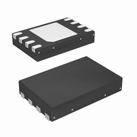
SE97BTP,547 NXP Semiconductors, SE97BTP,547 Datasheet - Page 17

SE97BTP,547
Manufacturer Part Number
SE97BTP,547
Description
IC TEMP SENSOR DIMM 8HWSON
Manufacturer
NXP Semiconductors
Datasheet
1.SE97BTP547.pdf
(53 pages)
Specifications of SE97BTP,547
Package / Case
8-WSON (Exposed Pad), 8-HWSON
Function
Temp Monitoring System (Sensor)
Topology
ADC (Sigma Delta), Comparator, Register Bank
Sensor Type
Internal
Sensing Temperature
-40°C ~ 125°C
Output Type
I²C™/SMBus™
Output Alarm
Yes
Output Fan
Yes
Voltage - Supply
3 V ~ 3.6 V
Operating Temperature
-40°C ~ 125°C
Mounting Type
Surface Mount
Temperature Threshold
+ 150 C
Full Temp Accuracy
2 C
Digital Output - Bus Interface
I2C
Digital Output - Number Of Bits
11 bit
Supply Voltage (max)
3.6 V
Supply Voltage (min)
3 V
Description/function
Temperature Sensor
Maximum Operating Temperature
+ 125 C
Minimum Operating Temperature
- 40 C
Lead Free Status / RoHS Status
Lead free / RoHS Compliant
Lead Free Status / RoHS Status
Lead free / RoHS Compliant, Lead free / RoHS Compliant
Other names
568-5055-2
NXP Semiconductors
Table 6.
[1]
[2]
[3]
SE97B_1
Product data sheet
Command
Normal EEPROM read/write
Reversible Write Protection (RWP)
Clear Reversible Write Protection (CRWP)
Permanent Write Protection (PWP)
Read RWP
Read CRWP
Read PWP
The most significant bit, bit 7, is sent first.
V
A0, A1, and A2 are compared against the respective external pins on the SE97B. Do not apply V
Normal EEPROM read/write, Permanent Write Protection (PWP) and Read PWP.
I(ov)
ranges from 7.0 V to 10 V.
EEPROM commands summary
7.10.1.3 Acknowledge polling
7.10.2 Memory Protection
Acknowledge polling can be used to determine if the SE97B is busy writing or is ready to
accept commands. Polling is implemented by sending a ‘Selective Read’ command
(described in
acknowledge the slave address as long as internal write is in progress.
The lower half (the first 128 bytes) of the memory can be write protected by special
EEPROM commands without an external control pin. The SE97B features three types of
memory write protection instructions, and three respective read Protection instructions.
The level of write-protection (set or clear) that has been defined using these instructions
remained defined even after power cycle.
The memory protection commands are:
Table 6
This special EEPROM command consists of a unique 4-bit fixed address (0110b) and the
voltage level applied on the 3-bit hardware address. Normally, to address the memory
array, the 4-bit fixed address is ‘1010b’. To access the memory protection settings, the
4-bit fixed address is ‘0110b’.
sequence, respectively.
•
•
•
•
•
•
Permanent Write Protection (PWP)
Reversible Write Protection (RWP)
Clear Write Protection (CWP)
Read Permanent Write Protection (RPWP)
Read Reversible Write Protection (RRWP)
Read Clear Write Protection (RCWP)
is the summary for normal and memory protection instructions.
[3]
Section 7.10.3 “Read
Fixed address
Bit 7
1
0
0
0
0
0
0
Rev. 01 — 27 January 2010
[1]
Bit 6
0
1
1
1
1
1
1
Figure 13
DDR memory module temp sensor with integrated SPD
operations”) to the device. The SE97B will not
Bit 5
1
1
1
1
1
1
1
and
Figure 14
Bit 4
0
0
0
0
0
0
0
show the write and read protection
Hardware selectable
address
Bit 3
A2
V
V
A2
V
V
A2
SS
SS
SS
SS
I(ov)
to the A0 pin during
Bit 2
A1
V
V
A1
V
V
A1
SS
DD
SS
DD
© NXP B.V. 2010. All rights reserved.
Bit 1
A0
V
V
A0
V
V
A0
I(ov)
I(ov)
I(ov)
I(ov)
SE97B
[2]
[2]
[2]
[2]
R/W
Bit 0
R/W
0
0
0
1
1
1
17 of 53


