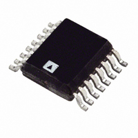
ADT7317ARQ-REEL Analog Devices Inc, ADT7317ARQ-REEL Datasheet - Page 19

ADT7317ARQ-REEL
Manufacturer Part Number
ADT7317ARQ-REEL
Description
IC SENSOR TEMP 10BIT DAC 16QSOP
Manufacturer
Analog Devices Inc
Datasheet
1.ADT7316ARQ.pdf
(44 pages)
Specifications of ADT7317ARQ-REEL
Rohs Status
RoHS non-compliant
Function
Temp Monitoring System (Sensor)
Topology
ADC, Comparator, Multiplexer, Register Bank
Sensor Type
External & Internal
Sensing Temperature
-40°C ~ 120°C, External Sensor
Output Type
I²C™, MICROWIRE™, QSPI™, SMBus™, SPI™
Output Alarm
No
Output Fan
No
Voltage - Supply
2.7 V ~ 5.5 V
Operating Temperature
-40°C ~ 120°C
Mounting Type
Surface Mount
Package / Case
16-QSOP
THEORY OF OPERATION
Directly after the power-up calibration routine, the ADT7316/
ADT7317/ADT7318 go into idle mode. In this mode, the device
is not performing any measurements and is fully powered up.
All four DAC outputs are at 0 V.
To begin monitoring, write to the Control Configuration 1
register (Address 0x18), and set Bit C0 = 1. The ADT7316/
ADT7317/ADT7318 go into their power-up default measure-
ment mode, which is round robin. The device proceeds to take
measurements on the V
sensor channel, and the external temperature sensor channel.
Once it finishes taking measurements on the external tempera-
ture sensor channel, the device immediately loops back to start
taking measurements on the V
cycle as before. This loop continues until the monitoring is
stopped by resetting Bit C0 of the Control Configuration 1
register to 0.
It is also possible to continue monitoring as well as switching to
single-channel mode by writing to the Control Configuration 2
register (Address 0x19) and setting Bit C4 = 1. Further explana-
tion of the single-channel and round robin measurement modes
is given in later sections. All measurement channels have averaging
enabled on power-up. Averaging forces the device to take an
average of 16 readings before giving a final measured result. To
disable averaging and consequently decrease the conversion
time by a factor of 16, set C5 = 1 in the Control Configuration
2 register.
Controlling the DAC outputs can be done by writing to the DAC
MSB and LSB registers (Address 0x10 to Address 0x17). The
power-up default setting is to have a low going pulse on the
LDAC pin controlling the updating of the DAC outputs from
the DAC registers. Alternatively, users can configure the updating
of the DAC outputs to be controlled by means other than the
LDAC pin by setting C3 = 1 of the Control Configuration 3
register (Address 0x1A). The DAC Configuration register
(Address 0x1B), and the LDAC Configuration register (Address
0x1C) can then be used to control the DAC updating. These
two registers also control the output range of the DACs, enabling
or disabling the external reference buffer, and selecting between
the internal or external reference. DAC A and DAC B outputs
can be configured to give a voltage output proportional to the
temperature of the internal and external temperature sensors,
respectively.
The dual serial interface defaults to the I
up. To select and lock in the SPI protocol, follow the selection
process as described in the Serial Interface Selection section.
The I
when selected, is automatically locked in. The interface can
2
C protocol cannot be locked in, while the SPI protocol,
DD
channel, the internal temperature
DD
channel and repeats the same
2
C protocol on power-
Rev. B | Page 19 of 44
only be switched back to be I
off and on. When using I
V
There are a number of different operating modes on the
ADT7316/ADT7317/ADT7318 devices, and all of them can
be controlled by the configuration registers. These features
consist of enabling and disabling interrupts, polarity of the
INT/ INT pin, enabling and disabling the averaging on the
measurement channels, SMBus timeout, and software reset.
POWER-UP CALIBRATION
It is recommended that no communication to the part is initiated
until approximately 5 ms after V
its final value. It is generally accepted that most systems take a
maximum of 50 ms to power-up. Power-up time is directly
related to the amount of decoupling on the voltage supply line.
During the 5 ms after V
bration routine; any communication to the device interrupts
this routine and can cause erroneous temperature measurements.
If it is not possible to have V
50 ms has elapsed, or that communication to the device has
started prior to V
measurement be taken on the V
ture measurement is taken. The V
calibrate out any temperature measurement error due to
different supply voltage values.
CONVERSION SPEED
The internal oscillator circuit used by the ADC has the capa-
bility to output two different clock frequencies. This means
that the ADC is capable of running at two different speeds
when performing a conversion on a measurement channel.
Thus, the time taken to perform a conversion on a channel
can be reduced by setting C0 of Control Configuration 3
register (Address 0x1A). This increases the ADC clock speed
from 1.4 kHz to 22 kHz. At the higher clock speed, the analog
filters on the D+ and D− input pins (external temperature
sensor) are switched off. This is why the power-up default
setting is to have the ADC working at the slow speed. The
typical times for fast and slow ADC speeds are given in the
Specifications section.
The ADT7316/ADT7317/ADT7318 power up with averaging
on. This means every channel is measured 16 times and inter-
nally averaged to reduce noise. The conversion time can also
be sped up by turning the averaging off; to do so, set Bit C5 of
the Control Configuration 2 register (Address 0x19) to 1.
DD
or GND.
DD
ADT7316/ADT7317/ADT7318
settling, then it is recommended that a
DD
2
C, the CS pin should be tied to either
has settled, the part performs a cali-
DD
2
C when the device is powered
at its nominal value by the time
DD
DD
DD
channel before a tempera
has settled to within 10% of
measurement is used to


