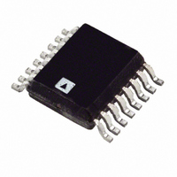
ADT7317ARQ-REEL Analog Devices Inc, ADT7317ARQ-REEL Datasheet - Page 37

ADT7317ARQ-REEL
Manufacturer Part Number
ADT7317ARQ-REEL
Description
IC SENSOR TEMP 10BIT DAC 16QSOP
Manufacturer
Analog Devices Inc
Datasheet
1.ADT7316ARQ.pdf
(44 pages)
Specifications of ADT7317ARQ-REEL
Rohs Status
RoHS non-compliant
Function
Temp Monitoring System (Sensor)
Topology
ADC, Comparator, Multiplexer, Register Bank
Sensor Type
External & Internal
Sensing Temperature
-40°C ~ 120°C, External Sensor
Output Type
I²C™, MICROWIRE™, QSPI™, SMBus™, SPI™
Output Alarm
No
Output Fan
No
Voltage - Supply
2.7 V ~ 5.5 V
Operating Temperature
-40°C ~ 120°C
Mounting Type
Surface Mount
Package / Case
16-QSOP
Writing to the ADT7316/ADT7317/ADT7318
Depending on the register being written to, there are two
different writes for the ADT7316/ADT7317/ADT7318. It is
not possible to do a block write to this part, that is, no I
auto-increment.
Writing to the Address Pointer Register for a Subsequent
Read
To read data from a particular register, the address pointer
register must contain the address of that register. If it does
not, the correct address must be written to the address pointer
register by performing a single-byte write operation, as shown
in Figure 51. The write operation consists of the serial bus address
followed by the address pointer byte. No data is written to any
of the data registers. A read operation is then performed to read
the register.
Writing Data to a Register
All registers are 8-bit registers so only one byte of data can be
written to each register. Writing a single byte of data to one of
these read/write registers consists of the serial bus address, the
data register address written to the address pointer register,
followed by the data byte written to the selected data register.
This is illustrated in Figure 52. To write to a different register,
another start or repeated start is required. If more than one byte
of data is sent in one communication operation, the addressed
register is repeatedly loaded until the last data byte is sent.
Reading Data from the ADT7316/ADT7317/ADT7318
Reading data from the ADT7316/ADT7317/ADT7318 is done
in a 1-byte operation. Reading back the contents of a register is
shown in Figure 56. The register address previously had been
set up by a single byte write operation to the address pointer
register. To read from another register, write to the address
pointer register again to set up the relevant register address.
Therefore, block reads are not possible, that is, no I
increment.
SDA
SCL
START BY
MASTER
Figure 52. I
1
1
0
2
C—Writing to the Address Pointer Register Followed by a Single Byte of Data to the Selected Register
SERIAL BUS ADDRESS BYTE
0
FRAME 1
1
SDA (CONTINUED)
SCL (CONTINUED)
A2
A1
2
C auto-
2
ADT7316/ADT7317/ADT7318
C
A0
ACKNOWLEDGE BY
Rev. B | Page 37 of 44
R/W
D7
9
1
D6
P7
1
SPI SERIAL INTERFACE
The SPI serial interface of the ADT7316/ADT7317/ADT7318
consists of four wires, CS , SCLK, DIN, and DOUT. The CS is
used to select the device when more than one device is connected
to the serial clock and data lines. The CS is also used to distinguish
between any two separate serial communications (see Figure 58).
The SCLK is used to clock data in and out of the part. The DIN
line is used to write to the registers and the DOUT line is used
to read data back from the registers. The recommended pull-up
resistor value is between 500 Ω to 820 Ω. Strong pull ups are
needed when serial clock speeds (which are close to the maximum
limit) are used or when the SPI interface lines are experiencing
large capacitive loading. Larger resistor values can be used for
pull-up resistors when the serial clock speed is reduced.
The part operates in slave mode and requires an externally
applied serial clock to the SCLK input. The serial interface
is designed to allow the part to be interfaced to systems that
provide a serial clock that is synchronized to the serial data.
There are two types of serial operations, a read and a write.
Command words are used to distinguish between a read and a
write operation, as shown in Table 58. Address auto-increment
is possible in SPI mode.
Table 58. SPI Command Words
Write
0x90 (1001 0000)
P6
D5
ADDRESS POINTER REGISTER BYTE
D4
P5
DATA BYTE
FRAME 3
P4
D3
FRAME 2
ADT7316/ADT7317/ADT7318
D2
P3
ADT7316/ADT7317/ADT7318
P2
D1
ADT7316/ADT7317/ADT7318
ACKNOWLEDGE BY
D0
P1
ACKNOWLEDGE BY
Read
0x91 (1001 0001)
P0
9
9
STOP BY
MASTER


