DC-VIDEO-TVP5146N Altera, DC-VIDEO-TVP5146N Datasheet - Page 16
DC-VIDEO-TVP5146N
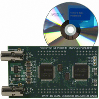
Manufacturer Part Number
DC-VIDEO-TVP5146N
Description
VIDEO DAUGHTER CARD
Manufacturer
Altera
Series
Stratix® IIIr
Datasheets
1.EP3SL150F780C4N.pdf
(16 pages)
2.EP3SL150F780C4N.pdf
(332 pages)
3.DC-VIDEO-TVP5146N.pdf
(58 pages)
Specifications of DC-VIDEO-TVP5146N
Main Purpose
Video, Daughter Card
Embedded
No
Utilized Ic / Part
Altera Dev Kits
Primary Attributes
Dual Composite Video Input - NTSC or PAL
Secondary Attributes
10-bit BT.656 Output, Compatible with Expansion Connector, Standard on Most Altera Development Kits
Lead Free Status / RoHS Status
Lead free / RoHS Compliant
Other names
544-1704


Table 1–20. PLL Specifications for Stratix III Devices (Part 3 of 3)
t
t
(7)
f
Notes to
(1) This specification is limited in the Quartus II software by the I/O maximum frequency. The maximum I/O frequency is different for each I/O standard.
(2) This specification is limited by the lower of the two: I/O f
(3) A high input jitter directly affects the PLL output jitter. To have low PLL output clock jitter, you must provide a clean clock source, which is less than 120 ps.
(4) F
(5) Peak-to-peak jitter with a probability level of 10
(6) High bandwidth PLL settings are not supported in external feedback mode.
(7) The cascaded PLL specification is only applicable with the following conditions:
(8) External memory interface clock output jitter specifications use a different measurement method and are available in
OUTCCJ_IO
DRIFT
CASC_OUTPJ_DC
Symbol
is applied.
a) Upstream PLL: 0.59 MHz Upstream PLL BW < 1 MHz
b) Downstream PLL: Downstream PLL BW > 2 MHz
REF
(5),
is fIN/N when N = 1.
Table
(5),
(8)
1–20:
Cycle to Cycle Jitter for clock
output on regular IO
(F
Cycle to Cycle Jitter for clock
output on regular IO
(F
Period Jitter for dedicated clock
output in cascaded PLLs (F
100 MHz)
Period Jitter for dedicated clock
output in cascaded PLLs (F
100 MHz)
Frequency drift after PFDENA is
disabled for duration of 100 s
OUT
OUT
100 MHz)
<100 MHz)
Parameter
–12
OUT
OUT
(14 sigma, 99.99999999974404% confidence level). The output jitter specification applies to the intrinsic jitter of the PLL, when an input jitter of 30 ps
max
or f
Min
—
—
—
—
—
out
of the PLL.
V
CCL
Typ
= 1.1 V
C2
—
—
—
—
—
Max
600
250
±10
60
25
Min
—
—
—
—
—
V
CCL
C3, I3
Typ
= 1.1 V
—
—
—
—
—
Max
600
250
±10
60
25
Min
—
—
—
—
—
Table 1–33 on page
V
CCL
C4, I4
Typ
= 1.1 V
—
—
—
—
—
Max
600
250
±10
60
25
1–29.
Min
—
—
—
—
—
V
CCL
Typ
= 1.1 V
—
—
—
—
—
Max
600
250
±10
60
25
C4L, I4L
Min
—
—
—
—
—
V
CCL
Typ
= 0.9 V
—
—
—
—
—
Max
32.5
750
325
±10
75
ps (p-p)
ps (p-p)
(p-p)
(p-p)
Unit
mUI
mUI
%
Related parts for DC-VIDEO-TVP5146N
Image
Part Number
Description
Manufacturer
Datasheet
Request
R

Part Number:
Description:
CYCLONE II STARTER KIT EP2C20N
Manufacturer:
Altera
Datasheet:


Part Number:
Description:
CPLD, EP610 Family, ECMOS Process, 300 Gates, 16 Macro Cells, 16 Reg., 16 User I/Os, 5V Supply, 35 Speed Grade, 24DIP
Manufacturer:
Altera Corporation
Datasheet:
Part Number:
Description:
CPLD, EP610 Family, ECMOS Process, 300 Gates, 16 Macro Cells, 16 Reg., 16 User I/Os, 5V Supply, 15 Speed Grade, 24DIP
Manufacturer:
Altera Corporation
Datasheet:
Part Number:
Description:
Manufacturer:
Altera Corporation
Datasheet:
Part Number:
Description:
CPLD, EP610 Family, ECMOS Process, 300 Gates, 16 Macro Cells, 16 Reg., 16 User I/Os, 5V Supply, 30 Speed Grade, 24DIP
Manufacturer:
Altera Corporation
Datasheet:
Part Number:
Description:
High-performance, low-power erasable programmable logic devices with 8 macrocells, 10ns
Manufacturer:
Altera Corporation
Datasheet:
Part Number:
Description:
High-performance, low-power erasable programmable logic devices with 8 macrocells, 7ns
Manufacturer:
Altera Corporation
Datasheet:
Part Number:
Description:
Classic EPLD
Manufacturer:
Altera Corporation
Datasheet:
Part Number:
Description:
High-performance, low-power erasable programmable logic devices with 8 macrocells, 10ns
Manufacturer:
Altera Corporation
Datasheet:
Part Number:
Description:
Manufacturer:
Altera Corporation
Datasheet:
Part Number:
Description:
Manufacturer:
Altera Corporation
Datasheet:
Part Number:
Description:
Manufacturer:
Altera Corporation
Datasheet:
Part Number:
Description:
CPLD, EP610 Family, ECMOS Process, 300 Gates, 16 Macro Cells, 16 Reg., 16 User I/Os, 5V Supply, 25 Speed Grade, 24DIP
Manufacturer:
Altera Corporation
Datasheet: