DC-VIDEO-TVP5146N Altera, DC-VIDEO-TVP5146N Datasheet - Page 28
DC-VIDEO-TVP5146N
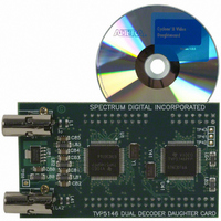
Manufacturer Part Number
DC-VIDEO-TVP5146N
Description
VIDEO DAUGHTER CARD
Manufacturer
Altera
Series
Stratix® IIIr
Datasheets
1.EP3SL150F780C4N.pdf
(16 pages)
2.EP3SL150F780C4N.pdf
(332 pages)
3.DC-VIDEO-TVP5146N.pdf
(58 pages)
Specifications of DC-VIDEO-TVP5146N
Main Purpose
Video, Daughter Card
Embedded
No
Utilized Ic / Part
Altera Dev Kits
Primary Attributes
Dual Composite Video Input - NTSC or PAL
Secondary Attributes
10-bit BT.656 Output, Compatible with Expansion Connector, Standard on Most Altera Development Kits
Lead Free Status / RoHS Status
Lead free / RoHS Compliant
Other names
544-1704


1–28
Table 1–29. Transmitter Channel-to-Channel Skew (TCCS)—Write Side
Table 1–30. DLL Frequency Range Specifications for Stratix III Devices
Stratix III Device Handbook, Volume 2
QDRII/II+ SRAM
QDRII/II+ SRAM
Emulation
RLDRAM II
RLDRAM II
Notes to
(1) The values apply to Column I/Os, Row I/Os, and Hybrid mode interfaces. Column I/Os refer to top and bottom I/Os. Hybrid mode refers to DQ/DQS groups
(2) For implementation, refer to the “Supporting ×36 QDRII+/QDRII SRAM Interfaces in the F780 and F1152-Pin Packages” section in the
Note to
(1) “Low” indicates a 6-bit DQS delay setting; “high” indicates a 5-bit DQS delay setting.
Frequency
Mode
wrapping over Column I/Os and Row I/Os of the device.
Interfaces in Stratix III Devices
0
1
2
3
4
5
6
7
Memory Type
Table
Table
(2)
1–30:
1–29:
120 – 200
150 – 240
180 – 300
240 – 370
290 – 450
360 – 560
470 – 740
90 – 150
C2
DLL and DQS Logic Block Specifications
Table 1–30
Frequency Range (MHz)
120 – 190
150 – 230
180 – 290
240 – 350
290 – 420
360 – 530
470 – 700
90 – 140
Standard
C3, I3
chapter.
1.8-V
HSTL
1.8-V
HSTL
1.5-V
HSTL
1.8-V
HSTL
I/O
lists the DLL frequency range specifications for Stratix III devices.
120 – 170
150 – 200
180 – 250
240 – 310
290 – 370
360 – 460
470 – 610
90 – 120
×9, ×18,
C4, I4
×9, ×18
×9, ×18
Width
×36
×36
120 – 170
150 – 200
180 – 250
240 – 310
290 – 370
360 – 460
470 – 610
90 – 120
C4L, I4L
Lead
259
279
290
259
V
TCCS (ps)
CCL
= 1.1 V
Chapter 1: Stratix III Device Datasheet: DC and Switching Characteristics
C2
Lag
276
296
278
276
Available Phase Shift
22.5°, 45°, 67.5°, 90°
60°, 120°, 180°, 240°
36°, 72°, 108°, 144°
36°, 72°, 108°, 144°
45°, 90°, 135°, 180°
45°, 90°,135°, 180°
30°, 60°, 90°, 120°
30°, 60°, 90°,120°
Lead
260
280
292
260
V
(Note 1)
TCCS (ps)
CCL
C3, I3
= 1.1 V
385
405
388
385
Lag
(Part 2 of 2)
Lead
280
300
315
280
V
TCCS (ps)
CCL
C4, I4
Delay Chains
= 1.1 V
Number of
© July 2010 Altera Corporation
Lag
418
438
421
418
16
12
10
12
10
8
8
6
Switching Characteristics
Lead
280
300
315
280
V
TCCS (ps)
CCL
C4L, I4L
= 1.1 V
Buffer Mode
DQS Delay
Lag
418
438
421
418
High
High
High
High
Low
Low
Low
Low
External Memory
Lead
380
400
415
380
V
TCCS (ps)
(1)
CCL
C4L, I4L
= 0.9 V
518
538
521
518
Lag
Related parts for DC-VIDEO-TVP5146N
Image
Part Number
Description
Manufacturer
Datasheet
Request
R

Part Number:
Description:
CYCLONE II STARTER KIT EP2C20N
Manufacturer:
Altera
Datasheet:


Part Number:
Description:
CPLD, EP610 Family, ECMOS Process, 300 Gates, 16 Macro Cells, 16 Reg., 16 User I/Os, 5V Supply, 35 Speed Grade, 24DIP
Manufacturer:
Altera Corporation
Datasheet:
Part Number:
Description:
CPLD, EP610 Family, ECMOS Process, 300 Gates, 16 Macro Cells, 16 Reg., 16 User I/Os, 5V Supply, 15 Speed Grade, 24DIP
Manufacturer:
Altera Corporation
Datasheet:
Part Number:
Description:
Manufacturer:
Altera Corporation
Datasheet:
Part Number:
Description:
CPLD, EP610 Family, ECMOS Process, 300 Gates, 16 Macro Cells, 16 Reg., 16 User I/Os, 5V Supply, 30 Speed Grade, 24DIP
Manufacturer:
Altera Corporation
Datasheet:
Part Number:
Description:
High-performance, low-power erasable programmable logic devices with 8 macrocells, 10ns
Manufacturer:
Altera Corporation
Datasheet:
Part Number:
Description:
High-performance, low-power erasable programmable logic devices with 8 macrocells, 7ns
Manufacturer:
Altera Corporation
Datasheet:
Part Number:
Description:
Classic EPLD
Manufacturer:
Altera Corporation
Datasheet:
Part Number:
Description:
High-performance, low-power erasable programmable logic devices with 8 macrocells, 10ns
Manufacturer:
Altera Corporation
Datasheet:
Part Number:
Description:
Manufacturer:
Altera Corporation
Datasheet:
Part Number:
Description:
Manufacturer:
Altera Corporation
Datasheet:
Part Number:
Description:
Manufacturer:
Altera Corporation
Datasheet:
Part Number:
Description:
CPLD, EP610 Family, ECMOS Process, 300 Gates, 16 Macro Cells, 16 Reg., 16 User I/Os, 5V Supply, 25 Speed Grade, 24DIP
Manufacturer:
Altera Corporation
Datasheet: