DC-VIDEO-TVP5146N Altera, DC-VIDEO-TVP5146N Datasheet - Page 7
DC-VIDEO-TVP5146N
Manufacturer Part Number
DC-VIDEO-TVP5146N
Description
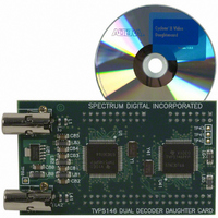
VIDEO DAUGHTER CARD
Manufacturer
Altera
Series
Stratix® IIIr
Datasheets
1.EP3SL150F780C4N.pdf
(16 pages)
2.EP3SL150F780C4N.pdf
(332 pages)
3.DC-VIDEO-TVP5146N.pdf
(58 pages)
Specifications of DC-VIDEO-TVP5146N
Main Purpose
Video, Daughter Card
Embedded
No
Utilized Ic / Part
Altera Dev Kits
Primary Attributes
Dual Composite Video Input - NTSC or PAL
Secondary Attributes
10-bit BT.656 Output, Compatible with Expansion Connector, Standard on Most Altera Development Kits
Lead Free Status / RoHS Status
Lead free / RoHS Compliant
Other names
544-1704


Chapter 1: Stratix III Device Datasheet: DC and Switching Characteristics
Electrical Characteristics
Table 1–8. On-Chip Termination Resistance Tolerance Specification for Stratix III Devices
© July 2010 Altera Corporation
R
25- R
25- R
25- R
50- R
50- R
50- R
R
OCT_UNCAL
D
S
S
S
S
S
S
Symbol
3.3, 3.0, 2.5
1.8, 1.5
1.2
3.3, 3.0, 2.5
1.8, 1.5
1.2
The accuracy listed in
temperature changes, the termination resistance value varies.
resistance tolerance for Stratix III OCT.
Table 1–9
calibration. Use
re-calibration.
Equation 1–1. OCT Variation Without Re-Calibration
Notes to
(1) R
(2) R
(3) T is the variation of temperature with respect to the temperature at power-up.
(4) V is the variation of voltage with respect to the V
(5) dR/dT is the percentage change of R
(6) dR/dV is the percentage change of R
Internal series termination without
calibration
Internal series termination without
calibration (25- setting)
Internal series termination without
calibration (25- setting)
Internal series termination without
calibration (25- setting)
Internal series termination without
calibration (50- setting)
Internal series termination without
calibration (50- setting)
Internal series termination without
calibration (50- setting)
Internal differential termination for
LVDS technology (100-setting)
V
CCIO
OCT
SCAL
Equation
.
value calculated from
is the OCT resistance value at power-up.
lists OCT variation with temperature and voltage after power-up
Description
1–1:
Table 1–9
Table 1–7
Equation 1–1
R
O CT
and
=
SCAL
SCAL
Equation 1–1
R
is valid at the time of calibration. If the voltage or
with temperature.
shows the range of OCT resistance with the variation of temperature and
with voltage.
SCAL
V
V
V
V
V
V
V
CCIO
CCIO
CCIO
CCIO
CCIO
CCIO
CCIO
1
= 3.3, 3.0, 2.5 V
= 1.8, 1.5 V
= 1.2 V
= 3.3, 3.0, 2.5 V
= 1.8, 1.5 V
= 1.2 V
= 2.5 V
CCIO
+
Conditions
at power-up.
dR
------ - T
dT
to determine OCT variation without
(Note 1)
dR
------ -
dV
V
Stratix III Device Handbook, Volume 2
—
±30
±30
±35
±30
±30
±35
Resistance Tolerance
C2
Table 1–8
-15 to 35
±40
±50
±60
±40
±50
±60
C3, I3 C4, I4
lists the
±40
±50
±60
±40
±50
±60
Unit
%
%
%
%
%
%
%
1–7
Related parts for DC-VIDEO-TVP5146N
Image
Part Number
Description
Manufacturer
Datasheet
Request
R

Part Number:
Description:
CYCLONE II STARTER KIT EP2C20N
Manufacturer:
Altera
Datasheet:


Part Number:
Description:
CPLD, EP610 Family, ECMOS Process, 300 Gates, 16 Macro Cells, 16 Reg., 16 User I/Os, 5V Supply, 35 Speed Grade, 24DIP
Manufacturer:
Altera Corporation
Datasheet:
Part Number:
Description:
CPLD, EP610 Family, ECMOS Process, 300 Gates, 16 Macro Cells, 16 Reg., 16 User I/Os, 5V Supply, 15 Speed Grade, 24DIP
Manufacturer:
Altera Corporation
Datasheet:
Part Number:
Description:
Manufacturer:
Altera Corporation
Datasheet:
Part Number:
Description:
CPLD, EP610 Family, ECMOS Process, 300 Gates, 16 Macro Cells, 16 Reg., 16 User I/Os, 5V Supply, 30 Speed Grade, 24DIP
Manufacturer:
Altera Corporation
Datasheet:
Part Number:
Description:
High-performance, low-power erasable programmable logic devices with 8 macrocells, 10ns
Manufacturer:
Altera Corporation
Datasheet:
Part Number:
Description:
High-performance, low-power erasable programmable logic devices with 8 macrocells, 7ns
Manufacturer:
Altera Corporation
Datasheet:
Part Number:
Description:
Classic EPLD
Manufacturer:
Altera Corporation
Datasheet:
Part Number:
Description:
High-performance, low-power erasable programmable logic devices with 8 macrocells, 10ns
Manufacturer:
Altera Corporation
Datasheet:
Part Number:
Description:
Manufacturer:
Altera Corporation
Datasheet:
Part Number:
Description:
Manufacturer:
Altera Corporation
Datasheet:
Part Number:
Description:
Manufacturer:
Altera Corporation
Datasheet:
Part Number:
Description:
CPLD, EP610 Family, ECMOS Process, 300 Gates, 16 Macro Cells, 16 Reg., 16 User I/Os, 5V Supply, 25 Speed Grade, 24DIP
Manufacturer:
Altera Corporation
Datasheet: